What is a Nanoindenter?
A nanoindenter is a versatile instrument used to test the mechanical properties of materials. Primarily developed for localized hardness testing, nanoindentation is now widely used to measure creep, fracture toughness, elastic modulus, stress relaxation, cracking, di slocation nucleation, and the viscoelastic properties of samples.
In this blog post, Alemnis explores the working principles of nanonindenters in more detail.
Nanoindenter Working Principles
At the heart of a nanoindenter is a small probe loaded with a calibrated indenter tip, which may be pyramidal, flat, spherical, wedged, or some other shape. This is used to interrogate the surface of a material and measure the subsequent force-displacement data.
Conventional nanoindenters are typically load-controlled instruments where the tip is brought into contact with the surface under a pre-defined load. Once the nanoindenter has contacted the sample, the load is increased and the tip indents into the material. The area of contact between the tip and the sample, the applied force of the nanoindenter, and the depth of displacement are subsequently used to determine the material’s mechanical properties. The disadvantages of a load-controlled system become obvious when doing compression tests on small structures (e.g., micropillars, 3D structures, etc.) where the load feedback loop cannot cope with sudden displacement excursions. In such cases, nanoindentation measurements using displacement control are far superior.
Traditionally, the size and depth of the residual indentation imprint is taken to calculate the material hardness. This is characterized according to one of several indentation hardness scales, including the Vickers and Brinell scales. Nanoindenters have proven valuable for microhardness testing where samples are small or thin, and they have also demonstrated unique performance for measurements where the microstructural properties of a sample are complex or are non-homogenous.

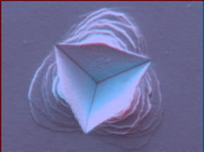
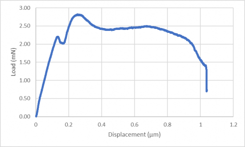
Typical example of a nanoindentation load-depth curve (left) and corresponding residual indent (right)
Applications of Nanoindentation Testing
Nanoindenters are broadly used to test the properties of hard coatings and thin films. As the dimensions of engineering and electronic components continue to decrease, it is vital that local mechanical properties are tested with very little residual impressions. Conventional techniques are largely incapable of testing small-scale components non-destructively, and in best case scenarios may impact the material properties of miniaturized components. Nanoindentation is subsequently used to characterize a range of materials to assist in research and development of new products and solutions. In the case of coatings, a nanoindenter can test the properties of even very thin films (e.g., thickness < 1 µm) without any influence from the properties of the substrate underneath.
Increasingly, nanoindentation has been used to test the complex properties of more dynamic material types including soft, hard, inorganic, and organic samples.
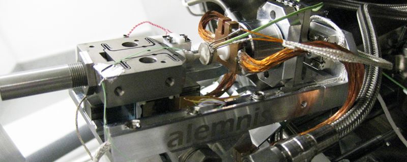
The Alemnis system is fully compatible for in-situ scanning electron microscopy (SEM) experiments, and ex-situ testing with Synchrotron beamlines and standard optical microscopes. This provides new levels of flexibility for dynamic material testing under high strain rates ( up to 10’000 s-1 ) and over very wide temperature ranges (from -150°C up to 1000°C)

Example of micropillar compression experiment with a flat punch diamond indenter
Localized mechanical testing of materials using the Alemnis system can provide new ways of understanding product failure under end-use conditions. It can be used to measure very small volumes of a specific material which can be in the form of a micropillar fabricated by focused ion beam (FIB) milling or by lithographic techniques such as LIGA. Small volume testing can help to understand the fundamental deformation mechanisms and if performed in-situ allows direct observation of the resultant phenomena, e.g. twinning or slip in metals, stress relaxation in ceramics or creep of oxide structures.
This level of precision has also been explored in the world of emerging biomaterials, offering new understandings of how tissues behave at a cellular level and how this behaviour can be modified. Quantitatively measuring the mechanical properties of biomaterials could provide new insights into biological behaviours, supporting research into innovative pharmaceuticals and medical devices. The Alemnis system can be used to do ex-situ bio-testing in various environments, such as controlled relative humidity, temperature or in liquids (e.g., saline or body-mimicking fluid).
The Unique Alemnis Solution
Alemnis is a specialist in small-scale mechanical testing for materials science research, with a nanoindentation system which can be used in either compression or tension modes. This means that a pillar can be compressed with a flat punch, a surface can be indented with a sharp indenter, or a microscale dogbone sample can be tensile tested, all with the same system. Such high versatility is unmatched and based on years of combined experience.
Read More: What Properties Can Be Measured by Nanoindentation?
The Alemnis system features a true displacement mode as well as various ultra-high strain rate options which permit strain rate jump tests, fatigue testing and dynamic mechanical analysis (DMA). Coupled with the latest state-of-the-art electronics and environmental control, the Alemnis system offers more versatility than any other.
If you would like to learn more about our nanoindenter systems, please do not hesitate to contact us directly.
What Properties Can be Measured by Nanoindentation?
Nanoindentation is a unique testing method used to assess various sample properties as a function of extremely small-scale surface deformation. Generally compact in design, nanoindentation systems can be utilized in a diverse set of applications for both organic and inorganic sample types. Biomaterials, ceramics, hard coatings, polymers, semiconductors, thin films, and more can routinely be analyzed using nanoindentation to determine numerous mechanical and dynamic characteristics.
In this blog post, Alemnis explores the properties that can be measured by nanoindentation.
Cracking and Fracture Toughness
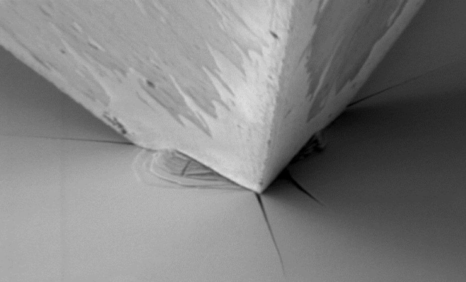
Nanoindentation of brittle solid materials like ceramics often causes lateral cracks to form around the impression. These may extend across the surface or nucleate beneath it, each of which can contribute towards important end-product phenomena. Cracking, particularly nucleation, is primarily indicative of a material’s fracture toughness.
Fracture toughness defines a material’s resistance to catastrophic failure when pre-existing flaws propagate through the product. Determining the fracture toughness of a given sample requires an understanding of its Young’s modulus and the dimensions of the defect. These are used to determine the stress intensity factor; a critical parameter for measuring the force per unit of surface area required for voids and cracks to propagate and cause materials to fail.
Nanoindentation measures Creep Deformation
Creep, or cold flow, is a measure of resistance to slow deformation in response to sustained mechanical stress. Nanoindentation can calculate the creep characteristics of a material by observing the increase in indenter tip depth as a function of time, as it is pressed into the sample surface at a constant force. This demands absolute precision and thermal stability of the nanoindentation system.
Nanoindentation detects Dislocation Nucleation
In materials science, dislocation nucleation occurs when the atomic bonds along a line in a lattice rupture due to shear forces. Homogenous dislocation nucleation requires many atomic bonds to break simultaneously which requires significant levels of shear stress. Nanoindentation is subsequently used to provide quantitative insights into material behavior at the onset of plasticity which is believed to contribute to dislocation, such as metal slipping or twinning.
Elastic Modulus and Hardness
Otherwise known as Young’s modulus, the elastic modulus of a material determines its resistance to deformation by compressive or bending forces. It is defined by the constant ratio of tensile stress to strain within the material’s elastic limits and can be used to calculate the applied tensile forces required for the material to plastically deform. The elastic modulus is intrinsically linked to both stiffness and hardness.
Nanoindentation was developed specifically for localized hardness testing of materials and has proven instrumental in testing their elastic moduli. As the elastic response of the surface sample is non-permanent, when the applied load of the nanoindenter tip is released, the sample surface will return to its original shape. Nanoindentation exceeds other hardness testing methodologies as it can also provide quantitative insight into elasticity.
Storage and Loss Moduli
Measuring the properties of viscoelastic samples with fixed geometries requires dynamic mechanical testing capable of acquiring storage and loss moduli. These refer to the measure of energy stored and lost in the elastic and viscous portions of the sample in response to linear stress. This is increasingly important for testing the properties of proprietary polymers and emerging biomaterials.
If you would like to learn more about the unique Almenis solution for nanoindentation testing, see our Product page
Nanoindentation with Alemnis
Alemnis specializes in small-scale mechanical testing for materials science research, offering a system equipped for both compression or tension modes. We can help you measure all the above properties and more.
Otherwise, contact us directly with any questions about our nanoindentation capabilities.
Selected references
- D. Tabor, Proc. R. Soc. A, 192 (1948) 247 (See article)
- M. F. Doerner, D. S. Gardner and W. D. Nix, J. Mater. Res., 1 (1986) 845-851 (See article)
- W. C. Oliver and G. M. Pharr, J. Mater. Res., 7 (1992) 1564-1583 (See article)
- N. X. Randall, R. Christoph, S. Droz, C. Julia-Schmutz, Thin Solid Films, 290-291 (1996) 348-354 (See article)
Which Indenter Materials are Best for High-Temperature Testing?
Nanoindentation and micro-compression tests are widely used to interrogate the mechanical properties of materials using either load or displacement control via an indenter tip of known geometry. This instrumented indentation principle has evolved from conventional methods of testing hardness, such as the Brinell or Vickers techniques and has emerged as the ideal candidate technology for evaluating a wide range of sample properties, such as hardness, elastic modulus, fracture toughness, creep, stress relaxation, strain rate sensitivity and slip deformation. However, material characteristics vary significantly with changes in temperature.
In some cases, the temperature dependence of material characteristics may have little-to-no implications for downstream applications. The same cannot be said of materials intended for use in thermal processing, refractory applications or as cutting tool coatings operating at high speeds and temperatures. Such materials must be characterized in simulated in-service temperatures, which can be challenging for conventional nanoindentation equipment.
In this blog post, Alemnis explores which nanoindenter materials are most suited for high-temperature testing.
Properties of High-Temperature Indenter Materials
Many of the challenges and quirks associated with assessing the mechanical properties of materials at elevated temperatures were first explored and overcome by hot hardness testing. This underlines many of the unique principles of high-temperature indentation. While indenter probes were initially chosen based on the highest possible hardness and stiffness, hot hardness tests demonstrated the importance of characterizing how these properties might change under test conditions.
Chosen indenter materials must retain their hardness at test temperatures, which often vary from room temperature up to 600°C (1112°F) in many industrial applications. Materials with poor coefficients of thermal expansion that exhibit exceptional hardness at room temperature may soften under test conditions. This can dramatically change the indenter area function, which in turn will cause an error in the subsequently calculated hardness or elastic modulus by a proportional amount. In addition, the indenter tip may become permanently damaged and lose its sharpness.
It is also important to assess mismatch in chemical reactivity between the indenter tip and the sample at high temperatures. Indenter materials that are inert at low temperatures may react with the sample material under test conditions, causing contamination of one or both materials in contact and, in extreme cases, dissolution of one material into the other.
Evaluating High-Temperature Indenter Materials
In order to perform a hardness test, the indenter material must be a minimum of 20% high hardness than the sample in order to generate plastic deformation. Ideally, the indenter should be > 100% harder in order to avoid rapid blunting or failure. A comprehensive analysis of high temperature indenter materials has been compiled by Wheeler and Michler (Ref. 1) and is shown in the hardness vs. temperature plot below. Although diamond is obviously one of the best indenter materials at ambient temperatures, its hardness decreases rapidly at elevated temperatures, although it still remains harder than all other candidates.
Diamond is the hardest engineering material available at all temperatures, from room temperature up to 1000°C (1832°F). It retains its exceptional intersection of mechanical properties throughout the most stringent high-temperature nanoindentation tests and remains the ideal solution for testing extremely hard materials like technical-grade ceramics and functional coatings. Cubic boron nitride (BN) is the next most noteworthy indenter material in terms of hardness at elevated temperatures, retaining its rigid structure up to operating temperatures of approximately 500°C (932°F) – after which it experiences an exponential drop in hardness.
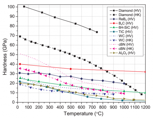
Hot Vickers and Knoop hardness of indenter materials as a function of temperature with extrapolated Vickers hardness shown as dotted lines for materials where only Knoop hardness data were available (from Ref. 1)
While not as hard as cubic boron nitride, tungsten carbide (WC) is significantly better at retaining its hardness at high temperatures, with a maximum peak operating temperature of approximately 900°C (1652°F).
However, as mentioned, these material properties are merely one aspect of indenter performance. The risk of cross-contamination between the indenter tip, the sample, and oxygen molecules in the atmosphere is significantly increased at elevated temperatures. Oxide formation on indenter tips is practically unavoidable when heated to temperatures exceeding 400°C (752°F), for diamond, boron nitride, and sapphire (Al2O3). Tungsten carbide is one of the least reactive indenter materials at high temperatures, which enables its application for high-temperature nanoindentation testing of metal alloys.
In many ways, the material of the indenter tip must be diagnosed with some understanding of the material under test. While diamond and tungsten carbide represent the ideal frontrunners in terms of maintained mechanical properties and low reactivity, there are always exceptions that disprove the rule.
Reactivity poses an additional issue in that it may impose a temperature limitation on many nanoindentation apparatuses, with an average maximum operating temperature in air of 200°C (392°F). This may be sufficient for proprietary tests, but it will not provide accurate insights into the material hardness of refractories and high-performance alloys. A typical solution to this is to conduct heated indentation tests in vacuum conditions.
High-Temperature Nanoindentation Testing with Alemnis
Alemnis offers a range of High Temperature (HT) modules for precision testing of samples with a heated nanoindentation tip up to 1000°C (1832°F). These retrofittable modules are compatible with all standard indenter tip materials which can be simply and easily exchanged between experiments.
If you would like to learn more about our high temperature modules for nanoindentation testing, please do not hesitate to contact Alemnis.
- J. M. Wheeler and J. Michler, Indenter materials for high temperature nanoindentation, Review of Scientific Instruments 84 (2013) 101301
How are Micropillars Produced?
How are Micropillars Produced?
Micropillar compression testing is a novel materials characterization technique that has emerged as a supplementary – and, in some instances, replacement – technology to indentation testing. Comparable to nanoindentation in terms of its ability to accurately quantify various mechanical properties of materials on the microscale, micropillar compression testing is a valuable addition to the technological arsenals of researchers concerned with myriad different sample types.
The underlying principles of these two techniques are similar, to the extent that near-identical instrumentation can be used to carry out both nanoindentation and micropillar compression tests. This has been demonstrated with materials as varied as metallic alloys, polymeric fibers, and refractory ceramics. The main advantage of micropillar compression over conventional nanoindentation is that the flat punch indenter maintains a constant contact area throughout the experiment so errors in area function are removed from the calculation of mechanical properties.
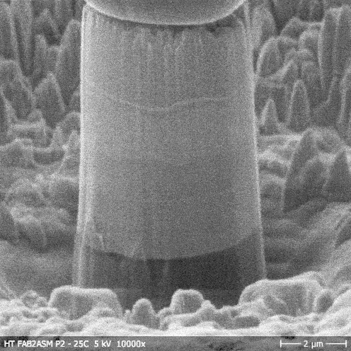
Example of a micropillar compression test on a micropillar built from a multilayer stack of different coatings
Outlining Micropillar Compression Testing
In a typical micro-compression test, a micrometer-scale (μm) pillar of sample material is compressed in a nanoindenter with a calibrated flat punch probe rather than a tip with a pyramidal geometry. Due to the extremely small dimensions of the micropillar, it is desirable to perform in situ positioning of the probe tip within the chamber of a scanning electron microscope (SEM). This eliminates errors associated with poor tip-optic calibration in ex situ testing conditions – yet it is not always appropriate to measure the deformation characteristics of materials in an SEM chamber. Certain polymers, for example, cannot be tested in the vacuum conditions of an SEM due to the potential for beam damage and cracking. In such instances, micropillar compression tests can be conducted in air under an optical microscope.
Each of these test methodologies can provide accurate insights into the real-world stress-strain properties of materials, including extremely complex behaviors like elastic moduli and microscale spatial variation of fracture toughness. Before these tests can be conducted, however, micropillars must be extracted from the bulk material.
Micropillar Fabrication
The primary method used to produce micropillars from bulk materials is focused ion beam (FIB) milling; a technology that mirrors the apparatus of a standard SEM array. Instead of a focussed beam of electrons, FIB setups utilize a high-energy gallium (Ga) ion beam to sputter the uppermost atomic layers of a material and facilitate ultra-precise sample machining on the sub-microscale. This process has become popularised in recent decades due to its outstanding accuracy in semiconductor etching applications.
Surface damage and implantation is a side-effect of FIB milling that could introduce measurement inaccuracies to micropillar compression tests. While gallium ion sources at high ion currents are desired for their superior top-down material removal rates, it may be necessary to ramp down the ion current during processing to optimize the structural and surface finish properties of the micropillar. This improves the yield of microscale samples with mechanical properties representative of the bulk material and decreases the likelihood of FIB induced damage that could affect compression results.
One of the disadvantages of FIB milling is that the micropillar in some materials may not have the same diameter over its whole length. An alternative is to fabricate micropillars from lithographic techniques where material is etched away after creating a surface mask. The advantage of lithographic techniques is that large arrays of micropillars can be fabricated in a few simple steps and much faster than by FIB milling. The shape of such pillars may also be more uniform. Some casting techniques are also available for producing micropillars, but then are based on the materials deposited rather than the bulk.
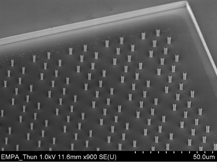
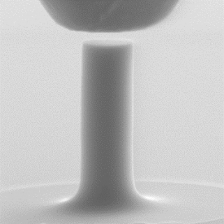
Examples of Si micropillar arrays (left) made by lithography and a single micropillar (right) just before contact with a diamond flat punch indenter.
Micropillar Testing with Alemnis
Alemnis specializes in the development of value-added tools and solutions for advanced materials testing studies and applications. Our versatile portfolio of products includes the industry-leading Alemnis Standard Assembly (ASA); a compact and flexible nanoindenter suitable for both nanoindentation testing and micropillar compression experiments.
For further information about performing next-generation materials testing with the Alemnis Nanoindenter, please do not hesitate to contact Alemnis today.

InnoSuisse HYSEMMEC project
Alemnis is proud to be an active partner in the InnoSuisse HYSEMMEC project. The proposed project aims to develop a new hybrid instrument that combines the high-resolution chemical and microstructural imaging of the table top SEM with the micro/nano mechanical testing capabilities of the Alemnis tester. This provides a unique opportunity for researchers from both academia and industry to have an automated stand-alone hybrid instrument that can be used for extended hours to provide correlated mechano-microstructural property maps with unprecedented temporal and spatial resolution. This requires miniaturization of the Alemnis product to fit the limited chamber space of the table top SEM, redesign of the support electronics, implementing the controller using FPGA technology, developing a GUI that can integrate operation of both the SEM and the mechanical test platform, establishing the software-hardware interface for automated high speed mechano-imaging of surfaces and finally adapting the Alemnis material analysis software to obtain automated post-processed modulus and hardness spatial maps.

Welcome Dr. Nicholas Randall
Alemnis is very pleased to welcome Dr. Nicholas Randall who joins as Vice President Business Development. He brings with him a solid business background combined with 25 years in the surface mechanical properties testing field.


INTERNATIONAL CONFERENCEON MANIPULATION; AUTOMATION AND ROBOTICS AT SMALL SCALES(MARSS)
1-5 July 2019
Helsinki, Finland
Dr. Nicholas Randall will be presenting a talk entitled “Recent innovation in the field of in-situ micro and nanoscale mechanical testing”