ELECTRON BACKSCATTER DIFFRACTION (EBSD)
The recent development of in situ mechanical testing in combination with direct observation and analysis is leading to an enhanced understanding of deformation mechanisms in materials. High resolution electron backscatter diffraction (HR-EBSD) straddles the mid-level resolution scale ( ̴ 100 nm) between studying individual dislocations in the Transmission Electron Microscope (TEM) and the bulk deformation behavior using techniques such as X-ray diffraction. One of the advantages of EBSD is that it is a surface technique and therefore is suitable for combination with a mechanical property testing technique such as nanoindentation, where the high spatial resolution is ideal for small-scale sample geometries.

Experimental arrangement for in situ EBSD mapping on a specific crystallographic plane during constant load segments
The example shows a typical experimental arrangement for micromechanical tests performed by nanoindentation on a micro-cantilever, a micro-pillar, and a micro-tensile sample, which have been fabricated on a mechanically and electro-chemically polished edge of a single crystal specimen using focused ion beam (FIB) milling. Samples of this type have final dimensions of ̴ 10 – 20 µm in length and 5-7 µm in thickness and width.
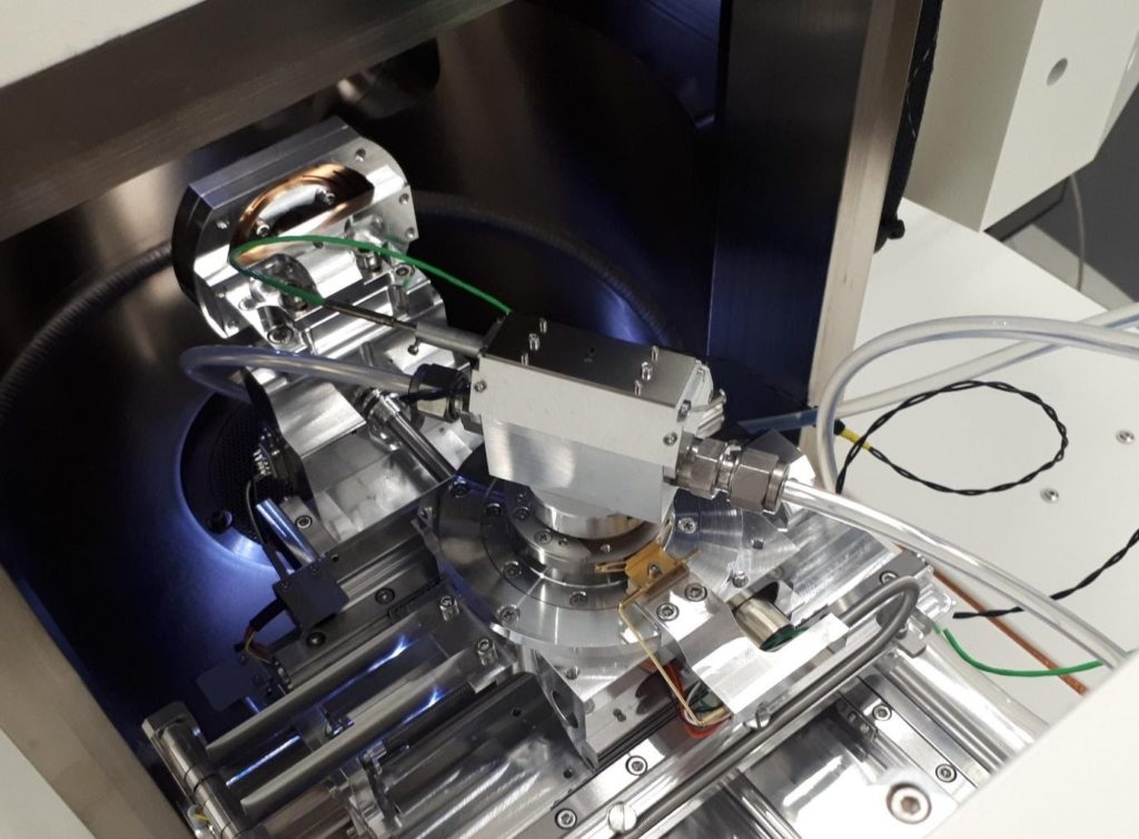
The sample and the indenter stage are aligned in such a fashion as to simultaneously perform micro-mechanical deformation tests with the indenter, visualize the experiment and acquire diffraction patterns using the EBSD detector. Typical test methodology on a cantilever beam comprises a displacement-controlled test with interrupted holds at various displacement steps, to collect diffraction patterns under loaded conditions. The cantilever surface facing the EBSD detector was the {100} plane in the example shown. Full displacement gradient tensors can be calculated from each EBSD scan, using a cross correlation software, such as CrossCourt 4.0 (BLG Vantage, UK) that allows determination of elastic strains with high strain sensitivity ( ̴ 2 x 10⁻⁴). Typically, 20 regions of interest with sizes of 128 x 128 pixels are selected on the recorded 2 x 2 binning Kikuchi patterns for the analysis. The elastic strains can be converted into stresses by applying the anisotropic Hooke’s law. The accumulated geometrically necessary dislocations (GND), created in the plastic regime, leave a measurable contribution to the local rotational gradient which can be determined with high angular resolution (10-4 rad).
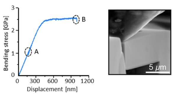
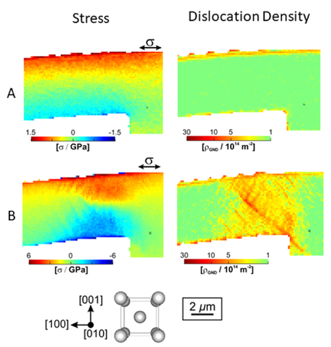
Example of a typical bending test (left) performed on a cantilever beam fabricated from single crystal tungsten. Point A shows the elastic portion of the deformation and point B the point of fracture. Corresponding EBSD diffraction data is shown (right) for stress and dislocation density
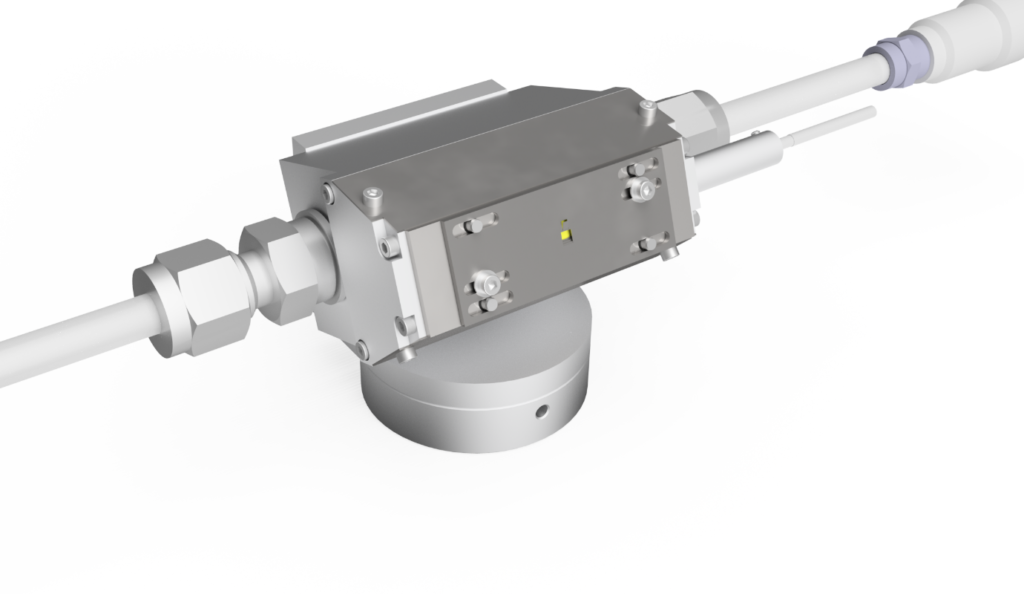
The Alemnis Standard Assembly (ASA) provides one of the only dedicated solutions for combining HR-EBSD with in situ micromechanical testing in a compact and user-friendly setup. Such a system can be applied to different material systems and loading geometries such as pillars, beams, tensile and shear specimen geometries. It can also be applied to complex microstructures where deformation mechanisms at interfaces, grain boundaries and precipitates are of interest. To summarize, HR-EBSD and in situ micromechanical testing are powerful complimentary analysis techniques that allow detailed investigation of the elastic-plastic deformation behavior of many materials at small scales.
NOTE: The Alemnis stage does not tilt because the EBSD is done immediately in situ, not post-mortem. This saves time and alleviates any need for repositioning. Flipping the sample is only good for post-mortem analysis, when it is much better to do it in-situ.
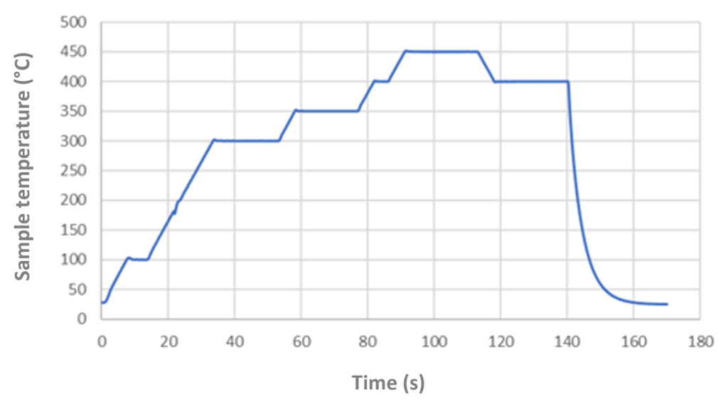
Alemnis also offers a dedicated heating stage specifically for EBSD analysis inside the SEM. The high temperature module for EBSD (HTME-1000) is a heating stage specifically designed for Electron Backscatter Diffraction (EBSD) analysis of a heated sample. It is not mountable on an Alemnis Standard Assembly (ASA) but is used freestanding in any SEM. It is designed for operation in vacuum and is optimized so that radiative heating of the sample is minimized at temperatures > 500°C to ensure the best possible EBSD analysis.
The HTME-1000 provides a compact and stable platform for EBSD studies over wide temperature ranges up to 1000°C and can accommodate samples of various thickness, although thin samples are favourable as they will reach thermal equilibrium faster.
Selected References
- J. Ast, G. Mohanty, Y. Guo, J. Michler, X. Maeder, In situ micromechanical testing of tungsten micro-cantilevers using HR-EBSD for the assessment of deformation evolution, Materials and Design 117 (2017) 265-266
- J. Ast, M. N. Polyakov, G. Mohanty, J. Michler, X. Maeder, Interplay of stresses, plasticity at crack tips and small sample dimensions revealed by in-situ microcantilever tests in tungsten, Materials Science & Engineering A, 710 (2018) 400-412
- Y. Guo, J. Schwiedrzik, J. Michler, X. Maeder, On the nucleation and growth of {1122} twin in commercial purity titanium: in situ investigation of the local stress field and dislocation density distribution, Acta Materialia 120 (2016) 292-301
- J. Wilkinson, T. B. Britton, Strains, planes and EBSD in materials science, Materials Today 15, No. 9 (Sept 2012) 366-376
- T. B. Britton and J. L. R. Hickey, Understanding deformation with high angular resolution electron backscatter diffraction (HR-EBSD) – IOP Conference Proceedings – Proceedings of EMAS-2017/IUMAS-7
- Niederberger, W. Mook, X. Maeder, J. Michler, Mater. Sci. Eng. A 527 (2010) 4306
- X. Maeder, W. Mook, C. Niederberger, J. Michler, Philos. Mag. 91 (2011) 1097