Understanding the Different Types of Extreme Conditions Tests
When a material is used for a specific application, an expectation is created around why it has been chosen. These assumptions will be based on the durability of its properties and characteristics. The reliability of materials make all the difference when facing a dangerous situation. Therefore, extreme conditions tests must be conducted on materials to ensure their suitability and dependability.
Now, extreme conditions tests look into all aspects of a material. It considers its structure, as well as its advantages and weaknesses. Extreme conditions tests can also ensure that the material adheres to different specifications and regulations.
Some tests may focus on extreme temperatures. Others may study the rate that a material will deteriorate or collapse under pressure. These are only a few examples of the extreme conditions tests that can be applied to materials to regulate their functionality, reliability and protective capabilities.
With that said, let’s explore these extreme conditions tests further. That way you can learn about extreme conditions testing, and potentially use them to study the properties of your own materials.
High-Temperature Testing
High-temperature testing examines how materials behave when exposed to temperatures that may reach or exceed their operational limits. These extreme conditions tests are critical for materials used in environments where high heat is a constant factor. This includes jet engines and power plants. The goal is to determine a material’s thermal stability, oxidation resistance, and mechanical strength at elevated temperatures.
Low-Temperature/Cryogenic Testing
Conversely, low-temperature or cryogenic testing assesses material performance at extremely low temperatures, often nearing absolute zero. This testing is vital for applications in outer space, where materials must withstand the vacuum and cold of space, and for the storage and transport of cryogenic substances. Under these conditions, materials are evaluated for their:
- Brittleness
- Thermal contraction
- Mechanical properties.
High Strain Rate Testing
Materials often need to absorb or resist high-impact forces rapidly in automotive and military applications. High strain rate testing investigates how materials deform or fail when subjected to rapid loads or impacts. These types of extreme conditions tests help to understand the dynamic behavior of materials. They are crucial for developing products that require high impact resistance, such as:
- Helmets
- Car bumpers
- Protective gear.
Corrosion Testing
Materials exposed to harsh chemical environments or extreme weather conditions are tested for corrosion resistance. Corrosion testing simulates these conditions to predict how materials will degrade over time. These extreme conditions tests are essential for ensuring the longevity and safety of structures and components in marine, chemical, and outdoor applications.
Radiation Testing
Radiation testing evaluates the effects of various types of radiation on materials, including:
- UV
- X-ray
- Gama
- Neutron radiation.
This testing is critical for materials used in nuclear reactors, space missions, and medical equipment, where radiation exposure is a concern. Extreme conditions tests can focus on radiation-related changes in relation to a material’s properties. These alterations could include the material’s:
- Strength
- Color
- Chemical resistance.
Pressure Testing
Pressure testing subjects materials to pressures above or below atmospheric levels to simulate deep-sea or high-altitude conditions. This type of testing is crucial for the following industries:
- Aerospace
- Underwater exploration
- Oil and gas.
In these areas, materials must withstand extreme pressure variations without failing.
Fatigue Testing
Fatigue testing is conducted to determine how materials behave under repeated or cyclic loading conditions. It simulates the wear and tear materials experience over time in applications like:
- Bridges
- Aircraft
- Machinery.
This testing helps identify the point at which materials may fail because of fatigue. By understanding fatigue, engineers can design more durable and reliable products.
Environmental Testing
Environmental testing includes extreme conditions tests that simulate a variety of environmental conditions. These include humidity, salt spray, sand and dust exposure and thermal cycling.
Ultimately, environmental testing assesses how external conditions affect materials’ physical and chemical properties, ensuring that products can endure their intended operational environments.
Ready to Apply Extreme Conditions Tests to Your Materials?
Extreme conditions tests provide answers to the toughest of questions about the safety and applicability of your materials. In the worst of situations, you would not want your materials to fail you. Therefore, it is important to use extreme conditions tests to learn if they are suitable for specific applications.
A variety of industries utilize extreme conditions tests to see how their materials would react in a dangerous situation. For instance, vehicle manufacturers and those in the aerospace industry use simulated crashes to see what would happen to materials during a destructive impact. This includes how much protection they could offer to anyone inside a vehicle.
By learning more about these material properties through extreme conditions tests, we can predict how they are going to react under specific situations. Right now, research is being conducted into creating ceramic and metallic compounds that can be used in harsh conditions. For these materials, extreme conditions tests are crucial to discovering more about them and where they are best applied.
Extreme Conditions Testing for Real-World Applications
Materials need to be fashioned to survive even the most harsh of conditions. That way when they are applied in the real-world, they can live up to expectations. You would not want materials obtained for cars to be fragile, the same way you would not want a material used in an electrical circuit to easily overheat. This is where extreme conditions testing can come into play to ensure materials can perform even in difficult environments.
So, you may be asking yourself, what extreme conditions are applied to materials? Well, the main purpose of extreme conditions testing is to understand if the design of a material, including its characteristics and mechanical properties, would suit a specific application. Therefore, it may be tested under extreme cold or heat, corrosion, chemicals, pressure or even radiation.
Extreme conditions testing can be used to improve the properties of a material. That way, we can ensure they have the appropriate reaction when they are applied to products and encounter the worst of conditions.
Join us as we undertake a deep dive of extreme conditions testing for materials. We will consider why these tests are so important and how they have been optimized to provide thorough results.
Variations of Extreme Conditions Testing
If you want to learn about the characteristics of materials, you can use extreme conditions testing to see how they react to certain environments. Processes utilized by extreme conditions testing include:
- Dynamic Mechanical Analysis (DMA): By using a DMA test, you can see how a material will react to different conditions, including temperature and stress. From there, it can examine the material’s tan delta, storage modulus and loss modulus. Utilizing a DMA instrument can even be used to learn about glass transition temperatures and molecular motions when heat is applied.
- High Temperature Mechanical Testing: The temperature control of a material can be ascertained through high temperature mechanical testing. This is extremely useful for materials that are going to be used in temperature dependent applications.
- Tensile Testing: To learn about a material’s flexibility, you can use tensile testing. Force is applied to the sample to see how long it can withstand it until it breaks. You can utilize this test to learn about the strength of a material.
- Nanoindentation: This is another technique used to understand a materials’ mechanical characteristics, including its toughness. Using an indenter, it measures how far it can enter the material. This gives an indication of its strength.
The Importance of Extreme Conditions Testing
Materials are the foundation of nearly all technological advancements, from aerospace engineering to electronics and beyond. Their performance under stress, strain, and temperature variations can significantly impact a product’s:
- Durability
- Efficiency
- Overall success.
Thus, undertaking extreme conditions testing provides essential data for:
- Predicting Material Behavior: Understanding how materials deform, fail, or react under extreme conditions helps predict their behavior in actual applications. This can lead to improved designs and selection.
- Innovating New Materials: Data from extreme conditions testing can inspire the development of new materials with enhanced physical properties. Characteristics include increased strength, durability, or heat resistance.
- Ensuring Safety and Reliability: Testing ensures that materials will not fail unexpectedly. This could pose risks to safety and operational integrity in critical applications like aerospace, nuclear power, and medical devices.
Technological Advancements in Extreme Conditions Testing
Recent technological advancements have significantly improved the capabilities of extreme conditions testing.
State-of-the-art equipment allows for the detailed analysis of material properties at the micro and nano-scale. This level of detail is crucial for industries where the smallest imperfections can lead to catastrophic failures.
- High-Temperature Testing: Examining material behavior at temperatures that can reach up to 1000°C. It simulates conditions in jet engines, power plants, and other high-heat environments.
- Low-Temperature/Cryogenic Temperatures Testing: Testing materials at cryo temperatures as low as -150°C is essential for applications in space exploration, where materials must withstand the cold vacuum of space, and in the storage of liquefied gasses.
Cryogenic testing can use liquid helium during material evaluation because of its low boiling point. These types of cryogenic liquids are excellent for keeping materials cool. They can even be used to see how a material can react under tension and changes in temperature.
- Ultra-High Strain Rate Testing: Understanding material response to very high strain rates (exceeding 10,000/s) is critical for automotive and military applications. These applications require materials that can absorb high-impact forces within milliseconds.
Applications and Impact of Extreme Conditions Testing
The insights gained from extreme conditions testing have wide-ranging applications across various sectors:
- Aerospace and Defense: Ensuring the reliability of materials used in aircraft, spacecraft, and military hardware, which are regularly exposed to extreme environmental conditions.
- Automotive: Developing safer, more durable materials for vehicles, including those required for impact resistance in crashes.
- Energy: Enhancing the efficiency and durability of materials used in power generation and transmission, including those in nuclear reactors and renewable energy installations.
- Electronics: Innovating materials that can withstand the thermal and mechanical stresses experienced by electronic devices.
Ready to learn more about Extreme Conditions Testing?
Extreme conditions testing examines the reliability of materials. These tests make sure that when they are used they have the right characteristics to withstand difficult situations.
As we move into the future, extreme conditions testing will continue to improve. These improvements will help us enhance the accuracy of these tests. From there, we will be able to create even more precise material designs that can be applied to specific environments.
Not only that, but extreme conditions testing acts as an improvement indicator. If a material does not live up to expectations, we can understand why it has behaved in a certain way. This gives us room to enhance its design and performance for extreme conditions.
If you are interested in learning more, we invite you to look at our extreme conditions testing equipment. Here at Alemnis, we pride ourselves on being able to offer technology that can assist you with your research. This includes tools that can support your examination of materials and how they will react under extreme conditions testing.
Let us help you get the equipment you need for extreme conditions testing. That way you can ensure the accuracy and reliability of your results.
What is High Strain Rate Nanoindentation?
High strain rate nanoindentation is a sophisticated materials testing technique. It has emerged as a crucial tool for the mechanical characterization of materials at the nanoscale, particularly in understanding their mechanical properties under rapid deformation.
The methodology behind this technique extends the conventional nanoindentation process, which involves pressing a hard tip into a material to measure its mechanical properties. By incorporating high strain rates, this allows researchers and engineers to simulate and analyze conditions that materials might experience in high-speed impacts, explosions, or other dynamic events.
Below you will learn more about high strain rate nanoindentation. As well as this, you will find out about its advantages and how it is applied in different areas.
An Introduction to Nanoindentation
Nanoindentation, at its core, is a technique used to provide the mechanical properties of materials at the nanometer scale.
The tip of an indenter is small, sometimes as little as 10 nm, and sharp. When learning about the tip of the identors’ area function, fused silica can be used with it as a reference before an experiment is undertaken.
Applying nanoindentation involves using a controlled force on the surface of a material. Mechanical property measurements are then taken of the indenter’s penetration depth into the contact area. Sometimes flat punches are used as indenters to make the results of the process more visible.
This method provides precise measurements of hardness, elastic modulus, and other material properties at micro to nano scales. Traditional nanoindentation tests are typically conducted at relatively low strain rates, focusing on the quasi-static behavior of materials.
The Need for High Strain Rate Testing
The advent of high strain rate nanoindentation arose from the need to understand material behavior under rapid loading conditions. These conditions are relevant to numerous applications in the aerospace, automotive, defense, and electronics industries.
Materials subjected to high-speed impacts or rapid stress changes exhibit different properties than those measured under static conditions. High strain rate nanoindentation allows for the exploration of these dynamic responses. It offers insights into deformation mechanisms, fracture toughness, strain rate sensitivity, and phase transformations of materials under extreme conditions.
Methodology and Advancements
High strain rate nanoindentation is performed using specialized equipment capable of applying extremely rapid displacement of the indenter tip.
Recent advancements have introduced additional techniques:
- Piezoelectric actuators that can achieve high displacement rates
- High-speed data acquisition systems, which capture the transient responses of materials during indentation.
The indenter’s shape is chosen based on a specific material or the desired information. Usually it is a Berkovich indentation tip, a spherical tip, or a custom geometry,
One of the significant challenges in high strain rate nanoindentation is accurately measuring the mechanical response of materials. Namely, this is because of the short time scales involved. Advanced methodologies now include ultra-fast displacement and force sensing technologies, coupled with sophisticated data analysis algorithms, to accurately capture the material’s response.
Recent Advances in High Strain Rate Nanoindentation
High strain rate nanoindentation has witnessed significant advancements. Recent studies explore various materials, from microcrystalline cellulose to high-entropy alloys and structural steel, under extreme conditions.
These studies have employed innovative nanoindentation techniques to unravel the complex interplay between material properties, strain rate sensitivity, and deformation mechanisms.
Implications and Applications of High Strain Rate Nanoindentation
The insights gained from high strain rate nanoindentation are used across various fields, including in the examination of thin films.
For materials science, it aids in the development of materials with tailored properties for specific high-speed applications. Examples of this are protective gear, automotive components, and aerospace structures. Furthermore, understanding the dynamic behavior of materials at the nanoscale is critical for advancing nanotechnology applications, including nanoelectronics and nanocomposites.
High strain rate nanoindentation represents a critical advancement in the field of materials science. It offers a window into the dynamic behavior of materials under conditions that mimic real-world applications. Tensile tests are still useful for determining the yield properties of materials. However nanoindentation is much easier to use for sample creation.
As technology advances, the methodology continues to evolve, providing more detailed and accurate insights into material properties at the nanoscale. This technique not only enhances our understanding of material science but also drives innovation in designing materials and devices for future applications.
Are You Ready to Utilize High Strain Rate Nanoindentation?
As we navigate the intricate landscape of materials science, the significance of understanding and characterizing materials at the nanoscale cannot be overstated. High strain rate nanoindentation offers a window into the mechanical behaviors of materials under dynamic conditions. This is a crucial aspect for advancing technology and engineering materials for tomorrow’s needs.
For those poised to take their indentation testing methods and nanoindentation experiments to the next level, Alemnis provides state-of-the-art nanoindentation solutions. These are tailored for the precise determination of elastic modulus. They can also provide information about critical mechanical properties in a wide range of materials. We encourage you to explore the potential that Alemnis nanoindenters offer in pushing the frontiers of materials characterization. Learn more about how our nanoindentation technology can transform your research and contribute to groundbreaking discoveries by reading our detailed guide on determining elastic modulus with nanoindenters. Embrace the future of materials science with Alemnis at your side.
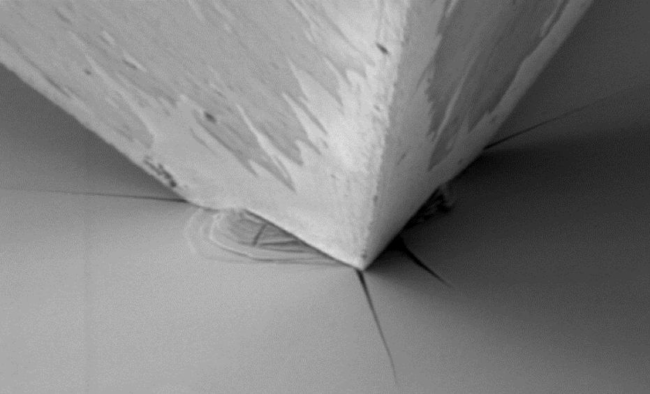
Conducting Surface Integrity Assessments via Scratch Resistance Testing
Scratch resistance testing is a mainstay in materials science. It has become increasingly vital for assessing the mechanical integrity of surfaces; particularly relevant for bulk materials and coatings. It is essential in various fields ranging from thin film analysis to micro-electromechanical systems (MEMS) development. This blog delves into scratch resistance tests’ methodology, applications, and significance in contemporary materials research and industrial R&D.
Scratch Test: A Versatile Assessment Tool
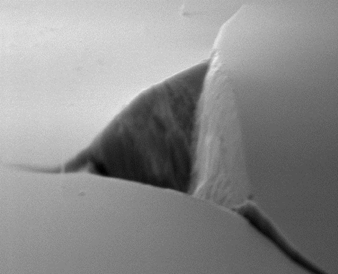
The scratch resistance test employs a meticulously designed indenter to apply a progressive load onto a material’s surface. This indenter, characterized by its specific geometric structure, is integral to the accuracy and reliability of the test. The geometry of the indenter, often a conical, spherical, or pyramid shape, is chosen based on the type of material and the specific properties being assessed.
As the indenter moves across the surface, it applies a controlled, increasing load. This graduated loading is crucial for methodically escalating the stress levels on the material. The progressive nature of the load allows for a detailed analysis of how the material behaves under different stress conditions. This gradual load increase leads to the test’s critical junctures: the failure events.
Failure events during a scratch resistance test are significant markers that provide a wealth of information about a material’s properties. These events may manifest as cracks, delamination, or complete coating detachment from the substrate. In soft materials, the concern is often about the indenter sinking into the material under excessive load. This sinking can skew the results by altering the stress applied to the material’s surface. Therefore, controlling and monitoring the load to avoid such occurrences is crucial to the scratch test.
The behavior of materials under these varying load conditions illuminates their adhesion and failure characteristics. For coatings, the test is particularly revealing, as it demonstrates how well a coating adheres to its substrate and under what conditions it begins to fail. This information is essential for predicting the coating’s behavior in real-world applications, where it may be subjected to various stressors.
Critical Load: The Point of Failure
A crucial aspect of scratch testing is identifying the ‘critical load’ – the normal load at which a surface fails. This load is a function of several factors, including coating adhesion, frictional stresses, and residual internal stresses within the coating. The critical load is not a static value but varies depending on the material properties and the applied conditions.
Observation Techniques
Scratch tests utilize various observation methods to analyze failure events. These include:
- Optical Microscopy: Provides a visual inspection of the surface and coating integrity.
- Acoustic Emission: Detects sound waves generated by crack formation or coating delamination.
- Frictional Force Measurement: Assesses the resistance offered by the surface during the test, indicating adhesion properties.
Applications in Materials Research and Industrial R&D
Scratch resistance tests have found widespread application in the analysis of:
- Thin Films: Assessing the durability and integrity of films used in various technological applications.
- Coatings: Evaluating surface coatings’ adhesion, hardness, and wear resistance.
- MEMS Devices: Investigating the mechanical properties of components in microsystems, crucial for ensuring reliability and performance.
The scratch resistance test is an indispensable tool in modern materials science, offering insights into the mechanical properties and failure mechanisms of various surfaces. Its adaptability and precision make it a standard method in both academic research and industrial product development.
Refer to our scratch testing page to learn more about how the Alemnis Standard Assembly (ASA) is used to conduct surface integrity assessments. Or, contact a member of the team today with any questions.
Understanding the Effects of Loading Rate in Nanoindentation Testing
Loading rates refer to the speed at which a nanoindenter applies force to a surface. It is instrumental in influencing the material’s mechanical response. Thus, loading rates help reveal time-dependent behaviour under stress. This helps researchers explain properties like elastic modulus, fracture toughness, hardness, etc. This blog post delves deeper into the recent research that illuminates the effects of loading rate in nanoindentation, focusing on diverse materials such as SU-8 polymer, microscale glass, and nanocrystalline nickel.
High Strain Rate Nanoindentation of SU-8 Polymer
In a groundbreaking study, Cherukuri et al. explored the mechanical properties of SU-8, a negative photoresist polymer essential in the fabrication of micro- to meso-scale structures, at high strain rates (up to 10^3 s^-1) using in situ micropillar compression and nanoindentation within a SEM environment. Their work highlighted the consistent mechanical properties of SU-8 across a wide range of strain rates, with no observable change in deformation mechanisms even at high strain rates. This is particularly noteworthy considering the SU-8 polymer’s extensive application in MEMS, where it’s exposed to various impact conditions. The researchers also introduced an innovative experimental protocol to minimize resonance amplitude during unloading, enabling the accurate extraction of modulus and hardness values using the Oliver-Pharr method.
Dynamic Plasticity and Failure of Microscale Glass
Ramachandramoorthy et al. conducted in situ high-strain-rate experiments on fused silica micropillars at strain rates up to 1335/s, observing a ductile-brittle-ductile transition in failure modes as strain rates increased. This study is crucial for understanding the dynamic mechanical properties of microscale glass, especially given its emerging role as a robust alternative to silicon in MEMS applications. The research revealed that at intermediate strain rates, the deformation in glass transitions through a serrated flow regime, characterized by the sequential propagation of individual shear bands. A transition to a more homogeneous deformation regime was observed at higher strain rates, attributed to the simultaneous nucleation of multiple shear bands and dissipative deformation heating.
Nanoindentation of Nanocrystalline Nickel
Schwiedrzik et al.’s nanocrystalline nickel (ncNi) study focused on its dynamic cryo-mechanical properties. They synthesized ncNi micropillars and complex micro-lattices using template-assisted electrodeposition and two-photon lithography, testing them at cryogenic temperatures and strain rates ranging from 0.001 to 500 s^-1. This research is pivotal in establishing microstructure-mechanical property relationships under extreme conditions, a necessity for the application-relevant design of metamaterials. Their findings showed minimal strain hardening and a low strain rate sensitivity in ncNi, which slightly increased at sub-ambient temperatures. This low strain rate sensitivity is critical for precision watchmaking applications and sensitive microsensors’ impact protection.
Learn more about nanoindentation testing with Alemnis
In sum, these studies collectively underscore the importance of understanding material behavior under varying strain rates, particularly in applications requiring high reliability and efficiency at the microscale. The advancement in high-strain rate nanoindentation testing techniques bridges the gap between theoretical knowledge and practical application. It contributes significantly to developing materials with tailored properties for specific industrial applications. This research is instrumental in paving the way for designing and optimising materials and devices that can withstand dynamic loading conditions, thus enhancing their performance and longevity in real-world applications.
The effects of loading rate in nanoindentation testing are multifaceted and significantly impact the mechanical characterization of materials. Dynamic mechanical analysis can help you understand the impact of stress and strain on a material. However, it is also crucial to have a basic understanding of the effects of loading rate. That way, you can produce an accurate material assessment.
This knowledge not only aids in predicting material behavior under different conditions but also in designing materials with tailored properties for specific applications.
At Alemnis, we recognize the critical role that nanoindentation testing plays in this journey. Our dedicated focus on expanding the frontiers of nanoindentation, particularly in challenging environments like high temperatures, addresses a wide range of material characterization needs.
Whether you are exploring the mechanical characterization of thin films, assessing the elastic recovery of novel materials, or delving into the time-dependent behavior of complex composites, Alemnis is your innovation partner. Our state-of-the-art equipment, optimized for various sample surfaces and sample preparation techniques, ensures precision and reliability. With our advanced indentation tip technology and the ability to control indentation depth accurately, we can reveal the intricate details of material behavior under varying applied forces.
We offer solutions that range from high-load applications to delicate, precision-focused tests. The displacement curves generated using our tools provide valuable insights into the rates that depend on material responses, facilitating comprehensive mechanical characterization.
At Alemnis, we are committed to pushing the boundaries of what’s possible in nanoindentation. To learn more about how our solutions can revolutionize your material testing capabilities, especially at high temperatures, visit us at Alemnis high-temperature nanoindentation. Discover a new dimension in material science where precision meets innovation.
References & Further Reading
1. Cherukuri, R. et al. Materials Letters 358 (2024) 135824.
2. Ramachandramoorthy, R. et al. Nano Lett. 2019, 19, 2350−2359.
3. Schwiedrzik, J. et al. Materials & Design 220 (2022) 110836.
Selecting the Right Nano Indenter Tips
A wide variety of nano indenter tips are available to choose from to assist you with any nanoindentation experiments.
Compared to traditional tests, nanoindentation is widely considered the gold standard for testing different surface mechanical properties. It involves using small probes and loads to produce smaller size indentation. This can be a few micrometers to a few hundred nanometers.
Selecting the most appropriate nano indenter tip is a crucial decision that can significantly impact the accuracy and reliability of your measurements during an indentation test. Choosing the right tips hinges on a nuanced understanding of the surface material’s mechanical properties. This includes its geometry, the material of the indenter tip, and its compatibility with the nanoindenter system.
This article elucidates the key considerations and options for choosing the right nano indenter tip for diverse applications.
Types of Nano Indenter Tips
When you think about the type of tip you want to perform nanoindentation with, you need to consider the characteristics of the materials you are going to analyze, as well as the tip’s indentation depth.
Additionally, you may want to consider how the tips will affect load displacement when analyzing how your material will change during the indentation test.
With that said, these are the nano indenter tips you should consider:
- Berkovich Tip:
The Berkovich tip is characterized by its three-sided pyramidal geometry. It has a 65.3° angle between the centerline and faces, and is adept for testing a wide range of materials. This includes bulk materials, thin films, and polymers.
This tip’s large included angle makes it particularly suitable for detailed mechanical characterization. That way it can understand elastic recovery and analyze fracture toughness when the tip and sample come into contact.
- Vickers Tip:
Featuring a four-sided pyramidal shape with a 68° centerline-to-face angle, the Vickers tip is versatile for testing bulk materials, films and foils. As well as this, it can be used for applications like scratch and wear testing. Its geometry offers a balance between penetration depth and surface interaction.
- Conical Tip:
The conical tip, with its sharp, self-similar geometry and cylindrical symmetry, is especially beneficial for modeling purposes. Its applications span across scratch testing, wear testing, imaging, and MEMS (Micro-Electro-Mechanical Systems) applications.
- Flat PunchTip:
This tip type, akin to the conical tip but featuring a flat end, is characterized by its cone angle and diameter. It finds its utility in various scenarios, such as scratch testing, wear testing, MEMS, and imaging.
- Other Tips:
For specific applications, such as thin films, cube-corner tips and wedge tips are also employed for surface contact. These specialized tips cater to unique material testing requirements.
Material Considerations
The choice of material for nano indenter tips is predominantly diamond and sapphire, known for their hardness and durability. These materials are available in various shapes. This includes sharp, flat, rounded, cylindrical, or spherical, to match specific testing requirements.
Advantages of Diamond Tips
- Exceptional Hardness: Diamond’s unparalleled hardness ensures the accurate and consistent measurement of material properties, like elastic modulus.
- High Thermal Conductivity: Diamond’s thermal conductivity is beneficial in minimizing thermal drift during testing, thereby enhancing result accuracy.
- Chemical Inertness: The chemical inertness of diamond reduces the risk of tip wear and sample surface contamination.
Which Nano Indenter Tips Would Work Best For You?
Selecting the right nano indenter tip is a nuanced process that necessitates a thorough understanding of the contact area of the material, as well as its properties, any testing requirements, and the indenter tip’s characteristics.
While diamond tips offer exceptional attributes like hardness, thermal conductivity, and chemical inertness, their anisotropy and cost for specific geometries are critical factors to consider.
Ultimately, the choice of selecting between nano indenter tips should be aligned with its specific application and the material properties of your project. That way you can ensure precise and reliable nanomechanical testing outcomes.
Key Advantages of Real-Time Contact Observation in Nanoindentation
Nanoindentation is a powerful technique for studying material properties at the nanoscale. Capable of measuring a range of metrics, nanoindentation has proven invaluable in fields from machinery engineering and electronics to implantology and agriculture.1 To enhance the effectiveness of nanoindentation, real-time contact observation has emerged as a key advancement. This article explores the concept of nanoindentation, highlights its importance, and discusses the advantages that real-time contact observation and high-temperature nanoindentation bring to the field.
Read more: Key Advantages of Real-Time Contact Observation in NanoindentationUnderstanding Nanoindentation
Nanoindentation is a versatile technique used to measure the mechanical properties of materials at the nanoscale. It involves the application of a controlled force on the surface of a material using an indenter, such as a spherical or pointed diamond and measuring the resulting penetration depth.2 The load-displacement data obtained during the process provides valuable insights into the material’s response to mechanical stress, offering a detailed understanding of its mechanical behavior. Properties such as hardness and elastic moduli can be assessed, and viscoelastic properties, fracture toughness and strain-hardening exponents can be derived.3
The Importance of Nanoindentation
In contrast to a microhardness tester, nanoindentation eliminates the need for a powerful microscope to measure the indentation impression. Instead, it relies on the indentation depth and the indenter geometry to determine the contact area. This characteristic makes nanoindentation particularly well-suited for examining nanoscale thin films and materials, as it allows for controlling the indentation depth to minimize substrate effects. These capabilities extend beyond the constraints of micro and macro tests, which can sometimes yield inaccurate measurements or only provide composite values, thereby making them particularly invaluable when dealing with coated materials or heterogeneous substances during testing.4
Advantages of Real-Time Contact Observation
Real-time contact observation takes nanoindentation techniques to new heights. Unlike conventional nanoindentation, the indentation area can be observed directly through an electron microscope allowing for the visualization of the contact area.5,6 This can lead to more reliable and repeatable experimentation. Furthermore, by viewing the indentation process, instantaneous feedback can be gathered on a material’s behavior, such as fracture onset, delamination, and time-sensitive behavior like viscoelasticity. Accordingly, researchers can identify changes in material properties that would otherwise be missed with conventional “post-mortem” analysis.7
Investigating High-Temperature Nanoindentation
High-temperature nanoindentation represents a specialized area within the field of nanoindentation, enabling precise characterization of a material’s mechanical behavior at elevated operational or processing temperatures. This involves subjecting the sample and indenter to temperatures as high as 800 °C, often conducted in a vacuum to prevent undesired atmospheric effects. The technique faces challenges like temperature drift and sample oxidation. However, with advancements like the Alemnis High-Temperature Module (HTM), high-temperature nanoindentation has become a standard method for studying temperature effects on material properties.8
Applications of Nanoindentation: High Temperature and Real-Time Contact Observation
High-temperature nanoindentation opens exciting possibilities for fundamental materials research. Its highly localized nature allows for an in-depth exploration of material behavior kinetics. This technique has been effectively employed to characterize a wide range of temperature-induced material effects, such as phase transitions in semiconductors like Si and Ge,9 stress-strain analysis of P91 steel,10 uncovering the atomic-level mechanisms of plasticity in solids,11,12 and crystallization behavior in bulk metallic glasses.13
High-temperature nanoindentation can also be combined with imaging techniques (e.g., SEM and TEM) and electrical measurements, enabling a comprehensive understanding of material behavior at the nanoscale.14 This has recently been demonstrated in additive manufacturing when investigating the temperature-dependent hardness of near-eutectic Ni-Nb,15 an Ni-based alloy that could be utilized in machinery components exposed to extreme loading conditions.16 Advances in these combined in-situ techniques permit real-time studies of temperature effects on microstructure and the intricate relationships between mechanical, electrical, and thermal phenomena at the nanoscale.[SL1]
Nanoindentation: A Small Measure with a Big Impact
Nanoindentation is a critical technique for understanding material properties at the nanoscale. Integrating real-time contact observation into nanoindentation techniques has significantly enhanced its effectiveness, allowing researchers to gain crucial insights into material behavior at unprecedented detail. With the development of high-temperature nanoindentation, the advantages of real-time observation hold immense promise for a wide range of applications in diverse industries. As research in this field continues to advance, real-time contact observation in nanoindentation will likely play a pivotal role in future materials science and engineering.
References and Further Reading
1. Nemecek J. (2012). Nanoindentation in Materials Science. http://dx.doi.org/10.5772/2829
2. Bhushan B, et al. (2016). Nanoindentation. Encyclopedia of Nanotechnology. https://doi.org/10.1007/978-94-017-9780-1_41
3. Peng Q. (2011). First-Principles Quantum Simulations of Nanoindentation. Nanoindentation in Materials Science. http://dx.doi.org/10.5772/48190
4. Sasmal S, et al. (2019). Nanoindentation for evaluation of properties of cement hydration products [chapter 7]. Nanotechnology in Eco-efficient Construction (Second Edition) Materials, Processes and Applications. https://doi.org/10.1016/B978-0-08-102641-0.00007-4
5. Cohen SR, et al. (2013). Dynamic nanoindentation by instrumented nanoindentation and force microscopy: a comparative review. Beilstein Journal of Nanotechnology. https://doi.org/10.3762/bjnano.4.93
6. Rzepiejewska-Malyska KA, et al. (2008). In situ mechanical observations during nanoindentation inside a high-resolution scanning electron microscope. Journal of Materials Research. https://doi.org/10.1557/JMR.2008.0240
7. Nowak J, et al. (2010). In-situ nanoindentation in the SEM. Materials Today. https://doi.org/10.1016/S1369-7021(10)70144-9
8. Alemnis [Online]. High Temperature Nanoindentation. Available at: https://alemnis.com/high_temperature_nanoindentation/ (Accessed on 27 July 2023)
9. Chavoshi SZ, et al. (2018). Temperature-dependent nanoindentation response of materials. MRS Communications. https://doi.org/10.1557/mrc.2018.19
10. Ruiz Moreno A, et al. (2020). Stress−strain curves and derived mechanical parameters of P91 steel from spherical nanoindentation at a range of temperatures. Materials & Design. https://doi.org/10.1016/j.matdes.2020.108950
11. Schuh CA, et al. (2005). Quantitative insight into dislocation nucleation from high-temperature nanoindentation experiments. Nature Materials. https://doi.org/10.1038/nmat1429
12. Choi I-C, et al. (2017). Thermally activated dislocation plasticity in body-centered cubic chromium studied by high-temperature nanoindentation. Acta Materialia. https://doi.org/10.1016/j.actamat.2017.08.026
13. Nieh TG, et al. (2004). Comparative studies of crystallization of a bulk Zr–Al–Ti–Cu–Ni amorphous alloy. Intermetallics. https://doi.org/10.1016/j.intermet.2004.04.011
14. Nili H, et al. (2013). In situ nanoindentation: Probing nanoscale multifunctionality. Progress in Materials Science. http://dx.doi.org/10.1016/j.pmatsci.2012.08.001
15. Jones MR, et al. (2023). Evidence of twinning-induced plasticity (TWIP) and ultrahigh hardness in additively-manufactured near-eutectic Ni–Nb. Journal of Material Science. https://doi.org/10.1007/s10853-023-08636-8
16. Vijay Reddy K, et al. (2020). Effect of Ni–Nb Metallic Glass on Moderating the Shock Damage in Crystalline Ni-Amorphous Ni62Nb38 Nanocomposite Structure: A Molecular Dynamics Study. In: TMS 2020 149th Annual Meeting & Exhibition Supplemental Proceedings. The Minerals, Metals & Materials Series. https://doi.org/10.1007/978-3-030-36296-6_85
Uncovering Small-Scale Fracture Mechanics with Nanoindenters
Fracture mechanics is an important branch of materials science that delves into understanding the cracks in materials and how they propagate. This field has been instrumental in predicting material failure, especially in engineering materials subjected to applied stress. As we venture deeper into the micro and nanoscale realms, the traditional methods of studying fracture mechanics often fall short. Enter nanoindentation – a technique that has revolutionised our understanding of material properties at these scales.
Nanoindentation: A Brief Overview
Nanoindentation experiments involve precisely applying a sharp indenter into a material’s surface. The resultant force-displacement curve offers a treasure trove of information, revealing the material’s elastic modulus, hardness, and other intrinsic mechanical properties. But beyond these basic metrics, nanoindentation has opened doors to the world of small-scale fracture mechanics.
Fracture Toughness and the Microscale Challenge
Fracture toughness is a material’s resistance to crack propagation. At the microscale, materials often exhibit behaviours distinct from their macroscale counterparts. Factors like plastic deformation, elastic-plastic transitions, and stress intensity factor variations at the crack tip become more pronounced. Traditional testing methods, rooted in linear elastic fracture mechanics (LEFM), may not always capture these nuances.
A Quick History of Fracture MechanicsFracture mechanics roots back to the late 19th Century. Back then, structural steel became brittle at around 20°C. This was a problem when high-volume steel production began in the 1860s. Engineers like David Kirkaldy noticed this issue, but it wasn’t a big problem because fractures were contained within individual plates. However, in 1898, there was a significant brittle fracture in a water standpipe in New York. The problem got worse with the introduction of electric arc welding. Welded structures, like the Vierendeel Truss Bridge in Belgium, started to fail. The most notable were the fractures in the welded Liberty Ships, leading to the establishment of committees to investigate the issue.Initially, brittle fracture was viewed mainly as a metallurgical issue. The focus was on determining the transition temperature from ductile to cleavage behaviour. The Charpy test was introduced to assess this transition temperature. The concept of size effect in brittle fracture emerged slowly, with the first fracture test simulating a welded plate structure developed by Wells. The issue was primarily addressed by developing steels with lower transition temperatures. However, later improvements to increase steel strength led to issues with fast ductile fracture in certain applications, which required the application of elasto-plastic fracture mechanics.
Fast forward to today, and the field has evolved, integrating advanced techniques like nanoindentation to study material properties at scales previously deemed challenging.
Interested in Small-Scale Fracture Mechanics?
At Alemnis, we’ve been at the forefront of these exciting developments. Our commitment to pushing the boundaries of understanding has led to innovations that are shaping the future of materials science. For those intrigued by the intricacies of fracture toughness and keen to delve deeper, we invite you to explore our dedicated resource on the subject. Discover a world where the micro meets the macro, and where every indentation tells a story.
References:
Cotterell, B. (2002). The past, present, and future of fracture mechanics. Engineering Fracture Mechanics 69. Available at https://imechanica.org/files/The%20past%2C%20present%2C%20and%20future%20of%20fracture%20mechanics_0.pdf
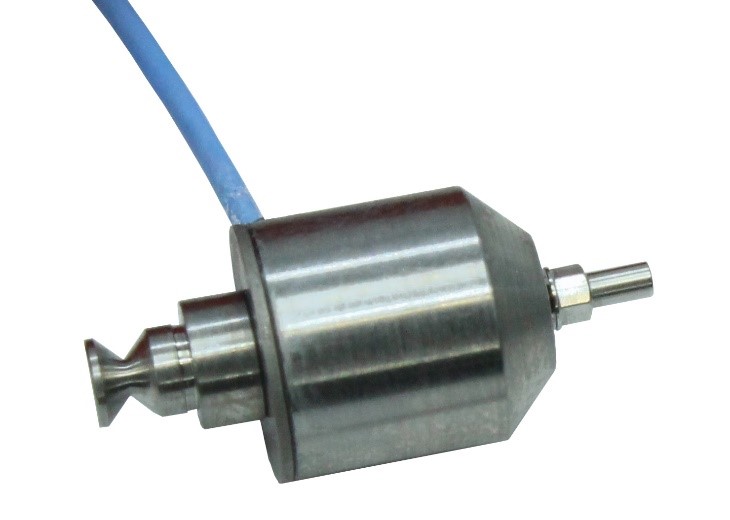
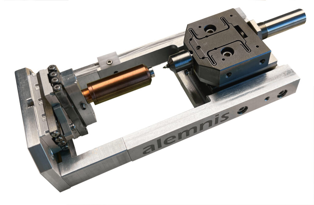
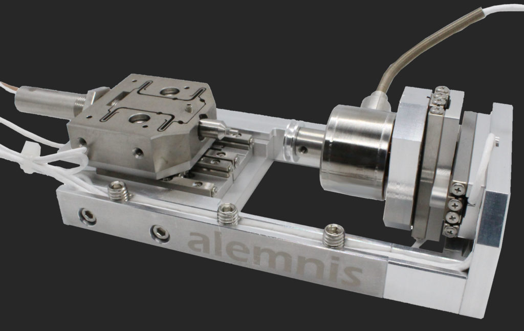
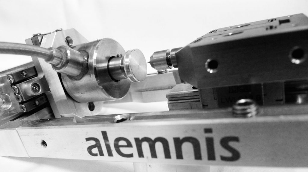
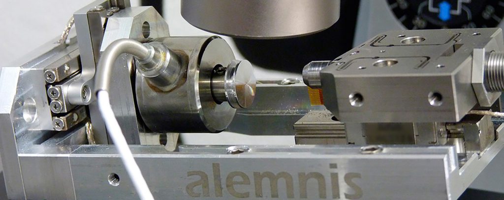
What are the advantages of the Alemnis mini load cell (MLC)?
The mini load cell (MLC) is a specialized device used to measure force or load. Its design and functionality are centered around precision and sensitivity, particularly in dynamically demanding applications. The “mini” aspect refers to its size compared to the Alemnis Standard Load Cell (SLC) making it suitable for applications where space is limited.
Working Principles of the Mini Load Cell
The Mini load cell ismeticulously designed to ensure precision and durability. The design of MLCs is intentionally compact lightweight and extremely stiff, facilitating their integration into various testing setups, especially where space is at a premium or when dealing with dynamic testing conditions.
At the heart of a mini load cell lies its critical component: the sensing element, which is usually a strain gauge. This gauge is a fine, conductive material that deforms slightly when subjected to a force. This deformation is crucial for the MLC’s function, as it is the primary data source for measuring the force. The strain gauge’s design and material composition are carefully calibrated to ensure responsiveness and accuracy in force detection.
The operation of an MLC revolves around the principle of deformation and electrical resistance. When a force is applied to the MLC, it causes the strain gauge to deform. This deformation, even though minute, results in a change in the electrical resistance of the gauge. This change is directly proportional to the magnitude of the force applied. The altered electrical resistance is then translated into an electrical signal through the MLC’s circuitry. This signal can be precisely measured and interpreted, clearly and accurately determining the force’s magnitude. The MLC’s ability to convert mechanical deformation into an electrical signal allows for high precision and reliability in force measurement, making it a vital tool in various scientific and engineering applications.
Features of Mini Load Cells
- High Precision and Sensitivity: MLCs can measure very small forcesin the micro-newton (µN) range. This high sensitivity makes them ideal for testing materials where slight variations in force can have significant effects.
- Dynamic Range: The Alemnis MLC works in an exterme range of forces from µN up to 4 N, which makes it ideally suited for testing comparably large structures or hard materials
- Small Size: The compact nature of MLCs allows them to be used in confined spaces and integrated into systems where larger load cells cannot fit.
- Versatility: They can be used in various applications, from biomechanical research to materials engineering. Their design allows for adaptations, such as different ranges of force measurement, to suit specific requirements.
- Robustness: Despite their small size, MLCs are durable and can withstand challenging environments, including changes in temperature, humidity, and exposure to chemicals.
Enhanced Precision and Sensitivity
Our mini load cells are engineered to provide exceptionally high precision in load measurement. With an applied load range starting from as low as 10 µN, these sensors can detect minute forces that are often critical in studying micro-scale materials. This high sensitivity is particularly beneficial for research in nanotechnology and microfabrication, where accurate force measurement is paramount.
Adaptability to Varied Testing Conditions
Combining MLCs with our Relative Humidity Module (RHM) allows tests to be conducted in highly controlled environmental conditions. This feature is crucial for experiments where relative humidity and temperature significantly impact material properties. It also facilitates testing in submerged conditions, broadening the scope of materials that can be studied, including hydrogels and biomaterials in simulated physiological environments.
Extended Load Range Flexibility
The standard load range of our MLCs, extending to 500 mN, can be expanded to 4 N by opting for alternative load sensors. This extended range is vital for a broader spectrum of material testing, encompassing everything from soft tissues to harder, more resilient materials. Such flexibility ensures that MLCs are confined to delicate materials and applicable in studying structural components.
Diverse Application Spectrum
The application range of mini load cells is remarkably diverse. In the realm of biomaterials, they are instrumental in understanding the mechanical properties of tissues and cellular structures. For micropillars and particles, MLCs facilitate the study of mechanical behavior under compression and tension. In gel testing, they allow for the examination of viscoelastic properties. Furthermore, their utility in tensile testing under various environmental conditions opens new avenues in material science research.
Advanced Data Acquisition and Analysis
Beyond physical versatility, MLCs by Alemnis are equipped with sophisticated data acquisition systems. This feature enables researchers to gather detailed, accurate data, which is crucial for advanced material analysis and modeling. The ability to accurately record and analyze load data paves the way for breakthroughs in understanding material behaviour under different stress conditions.
Elevate Your Material Testing Precision with Mini Load Cells
Are you looking to enhance the accuracy and scope of your material testing? Our mini load cells are engineered to deliver unmatched precision and adaptability in various testing environments. Explore our selection of standard and specialized MLCs to transform your material testing capabilities. Reach out to us now to discover more about how our load sensors can redefine precision in your testing processes.
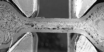
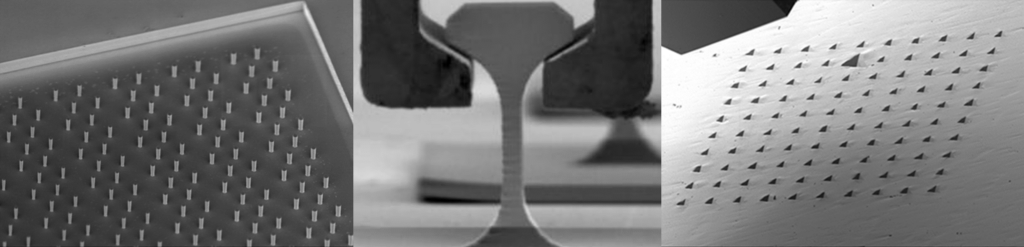
Understanding Material Strength Through Micro Tensile Testing
Material strength, a cornerstone concept in material science, dictates the ability of a material to endure external forces without collapsing or yielding. Micro-tensile testing is pre-eminent among tensile testing standards developed to gauge this intrinsic quality. It unlocks the ability to explore the tenets of a material’s strength at an almost atomic scale, offering insights often obscured at a macroscopic level.
The Science of Tensile Testing
Tensile testing, at its core, quantifies how a material reacts when subjected to stress.
Upon applying tensile stress, the first observed phenomenon is linear elasticity. It’s a regime where the material stretches but tends to revert to its original shape once the force dissipates. The gradient of the initial straight-line graph, the elastic modulus, serves as an index to how rigid or pliant a material is.
But as stress mounts, there arrives a point – the yield stress – beyond which the material won’t revert back. It has entered the realm of plastic deformation, where changes become irreversible. This stage is especially crucial in materials like metals, which can undergo significant deformation before snapping.
Ultimate Tensile Strength and Beyond
As one stretches the specimen, it reaches its ultimate tensile strength, the edge of its endurance. Past this point–though the material might still elongate–it becomes increasingly weaker until it fractures. The fracture strength denotes the exact stress level at which it gives way.
In micro tensile testing, the cross-sectional area plays a pivotal role in the determination of these strengths. Given the minuscule dimensions of the samples, even minor variances can influence outcomes, underscoring the precision required in sample preparation.
A Dive into Micro Tensile Mechanisms
The Alemnis Standard Assembly (ASA) system showcases the epitome of micro tensile testing machinery. The system offers an unparalleled insight into the intricacies of tensile strength and yield strengths at a microscopic level. By subjecting minute samples to stress, one can delineate the line between elastic and plastic deformations, capturing the nuances of material behaviour under strain.
Parallel to this, micropillar compression serves as a foil to tensile testing. Instead of stretching, these tiny pillars are subjected to compressive strength tests. By exploring both tensile and compressive domains, scientists can glean a comprehensive picture of the material’s robustness.
Lastly, in situ mechanical testing pulls back the curtain on real-time material reactions. Watching a material bend, stretch, and occasionally break, all while under a controlled environment, amplifies our understanding of its innate properties.
At Alemnis, we remain at the forefront of exploring material strengths, constantly endeavouring to expand the horizons of what’s known. Our commitment to refining techniques like micro tensile testing is unwavering. Such tests, along with their compression counterparts, grant invaluable insights into the very fabric of materials, from their elastic hopes to their plastic realities.
For those deeply entrenched in the realm of material science, or even those just kindling an interest, we invite you to explore more on tensile testing, its wonders, and intricacies.