SEMICONDUCTOR
The development of Integrated Circuit (IC) and other semiconductor devices has, in recent years, been more focussed on the fabrication process than on issues concerning reliability and the link to mechanical properties. Many issues related to tribology, mechanics, surface chemistry and materials science should be considered in the operation and manufacture of many devices.
A large proportion of modern semiconductor devices are made of silicon using complex manufacturing processes. As the applications of such devices increase, all classes of materials (metals, ceramics, polymers, composites) have become important. There are certain unique features of the mechanical properties of each class that require the testing procedures to vary from one to another. The properties considered to be important for the design of IC devices include the strength (yield, ultimate, fatigue), moduli, toughness, friction, adhesion, damping, Poisson’s ratio and residual stresses. From a manufacturing point-of-view, mechanical properties such as strength, hardness, scratch resistance and chemical-mechanical behaviour are important. The effect of the manufacturing procedure on the device properties also needs to be addressed. Properties such as crack propagation, friction, wear, fatigue, adhesion and property changes due to corrosion/oxidation/erosion during service will determine the lifetime of a device. Additionally, there is a growing demand for mechanical testing to be combined with electrical testing in the same platform so that a defined stress can be correlated to a change in electrical signal. See examples of electrical and mechanical testing here.
The Alemnis Standard Assembly (ASA) is a fully automated test platform which is dedicated to measuring the mechanical properties of highly localized areas of a system, whether discrete or as part of a wafer containing many thousands of devices. A wide choice of indenter geometries and test methods (indentation, scratch, tribology), coupled with SEM imaging make this modular solution the ideal choice for in-line characterization. The utilization of such an automated test platform on an IC production line allows a fast and efficient way of probing mechanical properties in a highly reproducible manner and in conformance with up-to-date ISO and ASTM standards.
Fast indentation mapping is a useful technique for mapping mechanical properties across predefined areas of interest. The Alemnis Automated Large Sample Platform (ALSP) can accommodate wafers up to 4 inch diameter, allowing any area of the wafer to be targeted. Indentation mapping is commonly used to test the properties of specific areas of bonding pads with unprecedented lateral positioning. This means that damaged areas (e.g., scrub marks from previous probe testing) can be avoided.
Example of fully automated mapping in 2 predefined zones of an aluminium-coated bonding pad.
Two 25 indent maps on either side of a scrub mark on an aluminium-coated bonding pad.
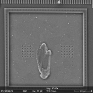
Specific testing of solder bump adhesion to the bonding pad is performed using an Alemnis Standard Assembly (ASA) equipped with a Lateral Force Sensor (LFS) and a custom made shear tip. The distance between tip and pad surface (typically 2 μm) is imposed at the beginning of the test and kept constant while applying a lateral displacement (typical rate of 0.5 μm/s) until the solder bump has been completely sheared away. The combination of SEM video and lateral load-displacement data provides a quantitative tool for subsequently calculating the interfacial shear strength.
Example of a bump-shear test of a single wire bonded solder bump showing delamination from the aluminium pad.
Specific semiconductor materials can be tested easily and quickly by fabricating micropillars locally on the wafer and subsequently testing their mechanical integrity by micropillar compression using a diamond flat punch indenter. Large arrays of micropillars can be built into the lithographic mask in “dead” regions which are not used for functional devices. This allows the mechanical properties of the actual materials used to be evaluated, thus providing a quality control tool which can detect variations across different areas of the wafer.
Fast micropillar compression mapping on a large array of Si micropillars of diameter 5.5 µm, height 15 µm and separation 75 µm.
Progressive load scratch testing is being increasingly used to evaluate the integrity and adhesion of surface coatings used in semiconductor manufacturing. In conventional scratch testing, a diamond stylus is drawn across the sample under either constant or progressively increasing load. Elastic and/or plastic deformation occurs at specific points along the scratch path, such critical points being observed by microscopy or by variations in frictional force. The driving forces for the failure of a coating-substrate system in the scratch test are a combination of elastic-plastic indentation stresses, frictional stresses and the residual internal stress present in the coating. The normal load at which failure occurs is called the critical load, Lc. When a progressive load scratch is performed, a number of consecutive coating failure events may be observed as the load is increased, the final event corresponding usually to total delamination. The critical load depends on coating adhesion, but also on several other parameters; some are directly related to the test itself (intrinsic parameters) whereas others are related to the coating-substrate combination (extrinsic parameters).
Example of a progressive load scratch test performed on an aluminium-coated semiconductor bonding pad. Normal load 1-24 mN applied on a spherical diamond indenter of radius 10 µm, with lateral speed 500 nm/s.