MICRO ELECTRO MECHANICAL SYSTEMS (MEMS)
The development of Micro Electro Mechanical Systems (MEMS) has, in recent years, been more focussed on the fabrication process than on issues concerning reliability and the link to mechanical properties. Many issues related to tribology, mechanics, surface chemistry and materials science should be considered in the operation and manufacture of many MEMS devices. At present, very few analytical instruments are available for accurate characterisation of localized properties and specific zones of interest. Instrumented indentation techniques provide a highly powerful method for measuring the load and depth response of bulk and coated materials, but can also be used to measure the mechanical properties of very small micro-machined silicon structures. Beam structures, such as are used for accelerometers, are a good example as they need to be characterised in terms of the number of cycles to failure, the spring constant or the energy required to bend the beam by a required amount. Such localised testing needs to be adapted to work at various distances from the origin of the beam with good positioning accuracy.
The indentation method for assessing mechanical properties at low loads and shallow depths is already well established for the characterisation of thin films as well as bulk materials. The depth-sensing indentation method produces a load-displacement curve from which quantitative property values can be calculated using a variety of approaches. Additionally, the indenter (of defined geometry) can be accurately controlled in terms of load, depth and speed of application. Provided that the indenter can be accurately positioned on a site of interest, then the technique can be used to probe the local mechanical properties of different structures, either with single or more complicated loading cycles.
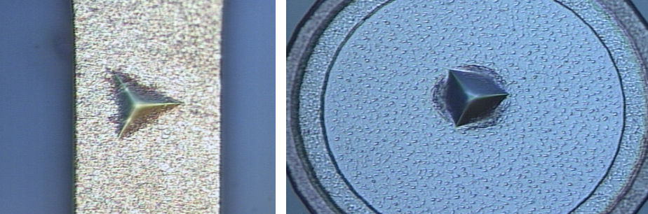
Examples of typical nanoindentations performed on bonding pads for MEMS devices
In addition to the quasi-static indentation method, where an indenter is moving solely in the vertical direction, the simple addition of an accurate displacement stage enables the sample to be moved horizontally, thus enabling a scratching function. In conventional scratch testing, a diamond stylus is drawn across the sample under either constant or progressively increasing load. Elastic and/or plastic deformation occurs at specific points along the scratch path, such critical points being observed in-situ or by optical microscopy, or by variations in acoustic emission and frictional force. In many cases, the scratch test has now become accepted as a versatile tool for assessing the mechanical integrity of a surface, whether bulk or coated, and has found application in many different fields of materials research. The driving forces for the failure of a coating-substrate system in the scratch test are a combination of elastic-plastic indentation stresses, frictional stresses and the residual internal stress present in the coating. The normal load at which failure occurs is called the critical load, Lc. When a progressive load scratch is performed, a number of consecutive coating failure events may be observed as the load is increased, the final event corresponding usually to total delamination. The critical load depends on coating adhesion, but also on several other parameters; some are directly related to the test itself (intrinsic parameters) whereas others are related to the coating-substrate combination (extrinsic parameters).
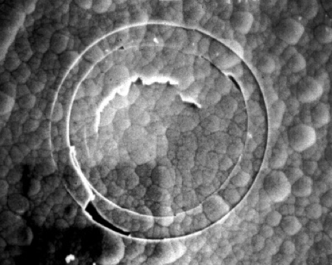

Example of ring cracks in a Diamond-like Carbon (DLC) coated MEMS device investigated using a 10 µm diameter spherical diamond indenter
A large proportion of modern MEMS devices are made of silicon using the manufacturing processes developed for integrated circuit production. As the applications of such devices increase, it is anticipated that all classes of materials (metals, ceramics, polymers, composites) will become important. There are certain unique features of the mechanical properties of each class that require the testing procedures to vary from one to another. The properties considered to be important for the design of MEMS devices include the strength (yield, ultimate, fatigue), moduli, toughness, friction, adhesion, damping, Poisson’s ratio and residual stresses. From a manufacturing point-of-view, mechanical properties such as strength, hardness, scratch resistance and chemical-mechanical behaviour are important. The effect of the manufacturing procedure on the device properties also needs to be addressed. Properties such as crack propagation, friction, wear, fatigue, adhesion and property changes due to corrosion/oxidation/erosion during service will determine the lifetime of a device. Since many microsystems are subjected to high frequency vibrations, damping and other dynamic properties, as well as fatigue, need to be accurately measured in order to simulate in-service conditions.
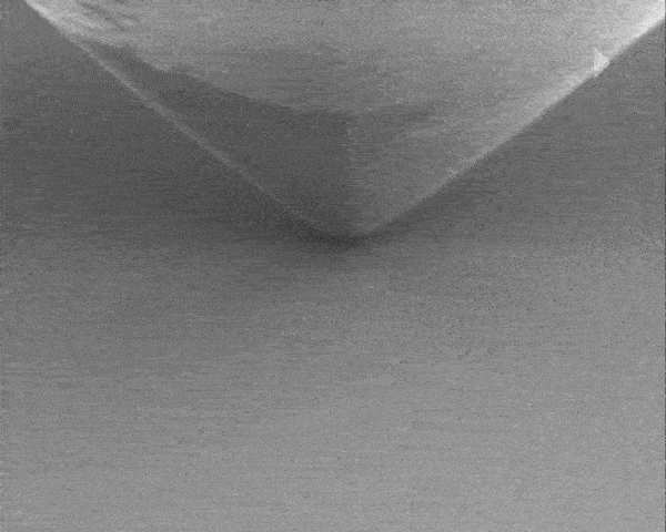
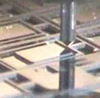
Typical fracture studies on Gallium Arsenide (GaAs) using a cube corner diamond indenter (courtesy of EMPA, Thun, Switzerland)
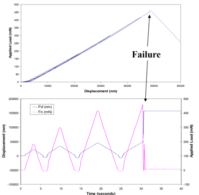
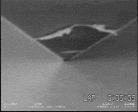
Indentation fatigue test on a MEMS beam using cyclic incremental loading until failure
The Alemnis Standard Assembly (ASA) can be used to perform standard nanoindentation fatigue tests (typically at low oscillation frequencies) or high frequency oscillatory fatigue tests with the Ultra High Strain (UHSR) option. The flexibility of the system allows fatigue testing to be performed in many sample orientations and configurations. Examples include quasi-static uniaxial indentation, high frequency indentation fatigue, beam bending, micropillar compression fatigue, impact fatigue, etc.
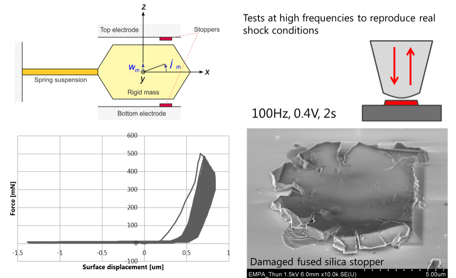
Simulation of a capacitive accelerometer stopper damaged by shock at high frequency