Automated Large Sample Platform

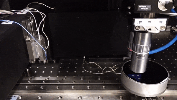
The Automated Large Sample Platform (ALSP) uses an ASA fitted with Mini Load Cell (MLC) together with an Extended XYZ Stage (EXYZ) and an Optical Microscope (OPT-MIC). The complete assembly fits inside the Insulating Enclosure (ENC-INS).

The EXYZ can accommodate samples up to 100 mm in diameter (including semiconductor wafers up to 4 inch diameter) with XY range of 150 mm, Z range of 30 mm, speed up to 15 mm/s and a blocking force of 5 N. The repositioning repeatability is < 500 nm over the entire travel range with a resolution (closed loop) of 1 nm.

Example of an Automated Large Scale Platform with custom optical microscope being used to characterize a 4 inch semiconductor wafer

Large scale mapping experiments are optimized with a unique tilt correction procedure which can be applied to the entire sample surface or portions of the surface, depending on the sample. Specific zones of interest can be defined to enable the most efficient Quality Control (QC) testing procedure. The ALSP can be used for a wide range of applications including semiconductor wafer mapping (e.g., bonding pads, MEMS structures, accelerometer beams, membranes, etc..), coatings, ternary thin film combinatorial libraries, etc.

Typical Quality Control (QC) test on a 4 inch wafer with 61 patches, 10 mm separation between patches. A 3 x 3 indent map is performed in the centre of each patch with an automated tilt correction performed for each wafer quadrant to optimize speed. Total number of indents is 549.