ELECTRICAL
A wide range of electrical applications are possible with the Alemnis Standard Assembly (ASA), ranging from electrical contact resistance measurements during material deformation to electro-chemical studies using the Liquid Cell (LIC).
The Liquid Cell (LIC) can be used for a wide range of experiments where the sample needs to be submerged in liquid. It is therefore typically used ex-situ with the Alemnis Standard Assembly (ASA) mounted vertically with the LIC mounted on the load cell. Some examples of how the LIC can be used are:
- Submerging biomaterials in saline solution or Body-Mimicking Fluid (BMF) to evaluate their mechanical properties when hydrated
- Electro-chemical tests where the indenter may be used as a current probe and the electrolyte (liquid) may be activated using an external potentiostat for corrosion or passivation studies
- Studies of hydrogel meso-porous effects, i.e. how the mechanical properties change as a function of the level of hydration.
- Tribological studies of interaction between the indenter and the sample when submerged in lubricant (liquid oil or grease), including tribo-corrosion experiments.
One example of a typical application of the LIC is the study of thin passive layers which can have significant effects on nanograin recrystallisation in tribological contacts. The LIC is optimized to allow a metallic sample to be indented at various electrochemical conditions by applying either passive or cathodic potentials in a suitable solution (e.g., 8.5 pH borate solution, made from an aqueous mixture of boric acid and sodium hydroxide). The liquid cell is converted into an electrochemical cell as shown. The sample is sandwiched between two polymer components with screws and a rubber O-ring provides a watertight seal while ensuring a reliable electrical contact between the sample and working electrode. The design thus allows for reusability between samples, variation in sample geometry and lateral movement of the indenter tip. The LIC is designed to contain approximately 1 ml of electrolyte solution. The working electrode is stainless steel with a 5 mm thickness of and 20 mm diameter, to which is soldered a wire. Four screws (M2) hold the top and bottom polymer components together. The rubber O-ring has an outer diameter of 12 mm and an inner diameter of 10 mm, thus defining the area of the sample in contact with the electrolyte solution. The entire cell is attached to the ASA with a single screw in the base.
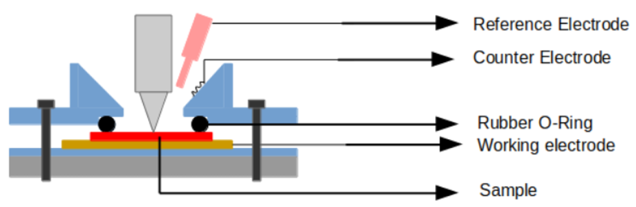
Schematic of Liquid Cell (LIC) used for electrochemical nanoindentation experiments
The Ag/AgCl reference electrode is connected to the cell through a bent glass capillary tube which is filled with the electrolyte solution. A thin platinum wire coil is inserted into the electrolyte as the counter electrode. Polarisation curves of the metallic sample materials are measured to determine the experimental values of potential for cathodic and passive surfaces. This typically consists of a single sweep from -2 V up to +2 V vs Ag/AgCl with a sweep rate of 0.05 V/s at room temperature.
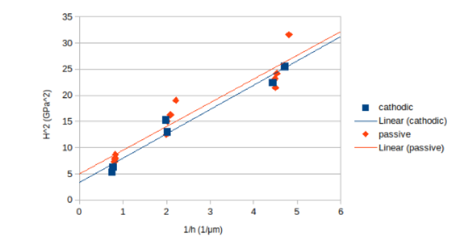
Depth (h) dependency of hardness (H) for indentations in Ni at cathodic and passive potentials
For electrochemical testing the indenter can also be used as a current probe. If this is the case, then an indenter of conducting material must be used (e.g., conductive diamond, tungsten carbide, etc.) together with an insulating holder. Alemnis can provide the Indenter Holder Insulating (IHI) for this purpose. The effects of performing indentation in the electrolyte solution are usually determined by performing indentations in the solution as well as on a dry sample. It is important to understand whether the load-depth curves vary between the two environments and also if there is any significant adhesive capillary effect at contact (this will depend on the surface area of the specific indenter used).
Some examples of indentations performed on a Ni sample are shown, one made at a cathodic potential of -1 V, the other at a passive potential of +0.5 V. In all cases, the potential is set and maintained for 10 minutes before indentation to allow for stabilization of the surface conditions. The AFM images shown here were made on the Ni surface after washing in an ultrasonic bath at room temperature for 30 s and then blow dried.
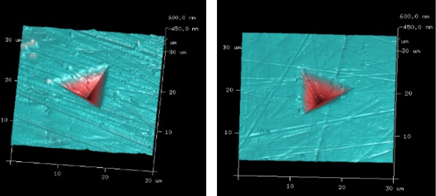
Example of 100 mN indents on Ni at cathodic potential (left) & passive potential (right)
Apart from electro-chemical tests performed with the LIC, the ASA is commonly used for making contact resistance measurements with a conducting indenter of defined geometry, or even with a tungsten probe. Several interesting studies have already been made to understand the effects of mechanical deformation in probe testing and the impact on the electrical signal. Some examples as follows:
- Use of a tungsten probe to simulate the probe testing process in microelectronics. The probe is loaded onto the surface of a bonding pad and the contact resistance monitored to investigate how much load is typically needed to overcome the surface oxide layer and achieve the best electrical continuity.
- Use of a tungsten probe to simulate the “scrub mark” or probe damage to the bonding pad. This can help to calibrate the actual probe test to minimize damage to the bonding pad.
- Nanoindentation of the bonding pad coating (commonly an aluminium coating of thickness ̴ 2 µm) to measure hardness and elastic modulus without any influence of the Si substrate.
- Lifetime studies to understand the change in electrical properties of the probe after many contact cycles. This can also be combined with fatigue testing at low or high cycles.
- Use of a tungsten probe to test individual PN junctions and detect failure.
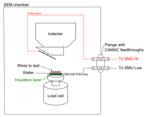
An example of the experimental setup for mounting a tungsten probe is shown, where external wires are brought directly to the probe and to the sample being tested. There is a great advantage to doing probe tests in-situ in the SEM, notably that the interaction between the SEM electron beam and the device being tested can be used to reveal information about defects. In addition, the ability to position a tungsten probe on an individual device with high positioning accuracy, provides a very powerful technique for failure analysis and/or rapid Quality Control (QC) inspection of individual microscale structures.
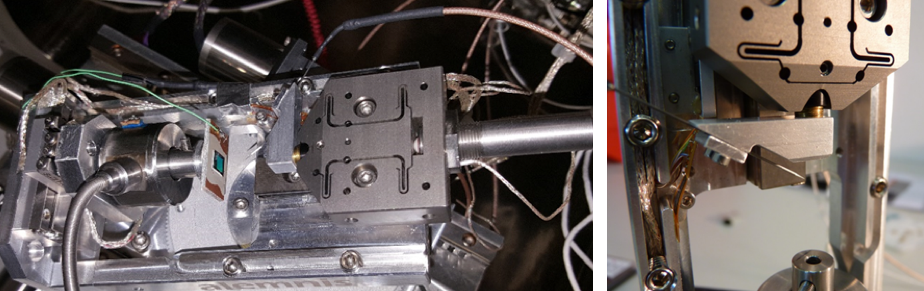
Modified ASA (left) for mounting tungsten wire for probe testing and detail (right) of the probe mounting.
Both Electron Beam-Induced Current (EBIC) and Electron Beam-Absorbed Current (EBAC) are interesting techniques for accurate single component investigation inside the SEM. Both require a rough localization of the defect by means of other techniques such as lock-in thermography. For example, a defective electrical transistor can show a reduced drain current in comparison to one which has full functionality. EBIC can determine the diffusion length of transistor PN junctions and so can be used to shed light on this anomaly and understand the root cause of the problem. The SEM electron beam induces electron-hole pairs which are separated by the internal electric field at the transistor PN junction, therefore creating an induced current which can be measured. The circuit diagram for PN junction probing with the ASA is shown, as well as how the external wires are routed through an SEM flange to an external Source Meter (e.g., Keithly 2400 SourceMeter SMU) which can simultaneously source and measure current from 10 fA to 10 A pulse and/or voltage from 100 nV to 1100 V, for 1000 W pulse and 100 W DC total power. The tungsten probe is brought into contact with a PN junction pillar and loaded up to a preset value, after which the resistivity measurements can be made. The influence of the applied load on the resistivity can also be evaluated.
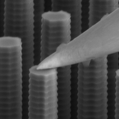
Circuit diagram (left) for in-situ probe testing in SEM and example of in-situ probe reliability test (right) on a PN junction (sample courtesy of Prof. A. Fontcuberta i Morral, EPFL-LMSC)
The combination of resistivity measurements with the EBAC technique provides a powerful means of characterizing metallic interconnects in integrated circuits (ICs). The electron beam of the SEM injects charges inside a certain interaction volume, such charges being absorbed by metal lines under the surface. A current is then induced and measured by the tungsten probe in contact at one end of the metal line of interest and the probed signal is overlaid on the secondary electron image, which enables easy detection of finely localized shorts and/or opens.
Selected References
- V. Nguyen, MSc Thesis, Effect of Passive Oxide Layer on Plastic Deformation of Metals during Nanoindentation, Ecole Polytechnique Federale de Lausanne (2016).
- M. Isard, I. Lahouij, P. Montmitonnet, J-M Lanot, Third body formation by selective transfer in a NiCr/AgPd electrical contact. Consequences on wear and remediation by a barrel tumble finishing, Wear 426 (2019) 1056-1064. https://doi.org/10.1016/j.wear.2018.11.022.