Understanding the Effects of Loading Rate in Nanoindentation Testing
Loading rates refer to the speed at which a nanoindenter applies force to a surface. It is instrumental in influencing the material’s mechanical response. Thus, loading rates help reveal time-dependent behaviour under stress. This helps researchers explain properties like elastic modulus, fracture toughness, hardness, etc. This blog post delves deeper into the recent research that illuminates the effects of loading rate in nanoindentation, focusing on diverse materials such as SU-8 polymer, microscale glass, and nanocrystalline nickel.
High Strain Rate Nanoindentation of SU-8 Polymer
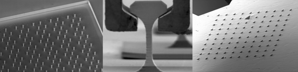
In a groundbreaking study, Cherukuri et al. explored the mechanical properties of SU-8, a negative photoresist polymer essential in the fabrication of micro- to meso-scale structures, at high strain rates (up to 10^3 s^-1) using in situ micropillar compression and nanoindentation within a SEM environment. Their work highlighted the consistent mechanical properties of SU-8 across a wide range of strain rates, with no observable change in deformation mechanisms even at high strain rates. This is particularly noteworthy considering the SU-8 polymer’s extensive application in MEMS, where it’s exposed to various impact conditions. The researchers also introduced an innovative experimental protocol to minimize resonance amplitude during unloading, enabling the accurate extraction of modulus and hardness values using the Oliver-Pharr method.
Dynamic Plasticity and Failure of Microscale Glass
Ramachandramoorthy et al. conducted in situ high-strain-rate experiments on fused silica micropillars at strain rates up to 1335/s, observing a ductile-brittle-ductile transition in failure modes as strain rates increased. This study is crucial for understanding the dynamic mechanical properties of microscale glass, especially given its emerging role as a robust alternative to silicon in MEMS applications. The research revealed that at intermediate strain rates, the deformation in glass transitions through a serrated flow regime, characterized by the sequential propagation of individual shear bands. A transition to a more homogeneous deformation regime was observed at higher strain rates, attributed to the simultaneous nucleation of multiple shear bands and dissipative deformation heating.
Nanoindentation of Nanocrystalline Nickel
Schwiedrzik et al.’s nanocrystalline nickel (ncNi) study focused on its dynamic cryo-mechanical properties. They synthesized ncNi micropillars and complex micro-lattices using template-assisted electrodeposition and two-photon lithography, testing them at cryogenic temperatures and strain rates ranging from 0.001 to 500 s^-1. This research is pivotal in establishing microstructure-mechanical property relationships under extreme conditions, a necessity for the application-relevant design of metamaterials. Their findings showed minimal strain hardening and a low strain rate sensitivity in ncNi, which slightly increased at sub-ambient temperatures. This low strain rate sensitivity is critical for precision watchmaking applications and sensitive microsensors’ impact protection.
Learn more about nanoindentation testing with Alemnis
In sum, these studies collectively underscore the importance of understanding material behavior under varying strain rates, particularly in applications requiring high reliability and efficiency at the microscale. The advancement in high-strain rate nanoindentation testing techniques bridges the gap between theoretical knowledge and practical application. It contributes significantly to developing materials with tailored properties for specific industrial applications. This research is instrumental in paving the way for designing and optimising materials and devices that can withstand dynamic loading conditions, thus enhancing their performance and longevity in real-world applications.
The effects of loading rate in nanoindentation testing are multifaceted and significantly impact the mechanical characterization of materials. Dynamic mechanical analysis can help you understand the impact of stress and strain on a material. However, it is also crucial to have a basic understanding of the effects of loading rate. That way, you can produce an accurate material assessment.
This knowledge not only aids in predicting material behavior under different conditions but also in designing materials with tailored properties for specific applications.
At Alemnis, we recognize the critical role that nanoindentation testing plays in this journey. Our dedicated focus on expanding the frontiers of nanoindentation, particularly in challenging environments like high temperatures, addresses a wide range of material characterization needs.
Whether you are exploring the mechanical characterization of thin films, assessing the elastic recovery of novel materials, or delving into the time-dependent behavior of complex composites, Alemnis is your innovation partner. Our state-of-the-art equipment, optimized for various sample surfaces and sample preparation techniques, ensures precision and reliability. With our advanced indentation tip technology and the ability to control indentation depth accurately, we can reveal the intricate details of material behavior under varying applied forces.
We offer solutions that range from high-load applications to delicate, precision-focused tests. The displacement curves generated using our tools provide valuable insights into the rates that depend on material responses, facilitating comprehensive mechanical characterization.
At Alemnis, we are committed to pushing the boundaries of what’s possible in nanoindentation. To learn more about how our solutions can revolutionize your material testing capabilities, especially at high temperatures, visit us at Alemnis high-temperature nanoindentation. Discover a new dimension in material science where precision meets innovation.
References & Further Reading
1. Cherukuri, R. et al. Materials Letters 358 (2024) 135824.
2. Ramachandramoorthy, R. et al. Nano Lett. 2019, 19, 2350−2359.
3. Schwiedrzik, J. et al. Materials & Design 220 (2022) 110836.
Selecting the Right Nano Indenter Tips
A wide variety of nano indenter tips are available to choose from to assist you with any nanoindentation experiments.
Compared to traditional tests, nanoindentation is widely considered the gold standard for testing different surface mechanical properties. It involves using small probes and loads to produce smaller size indentation. This can be a few micrometers to a few hundred nanometers.
Selecting the most appropriate nano indenter tip is a crucial decision that can significantly impact the accuracy and reliability of your measurements during an indentation test. Choosing the right tips hinges on a nuanced understanding of the surface material’s mechanical properties. This includes its geometry, the material of the indenter tip, and its compatibility with the nanoindenter system.
This article elucidates the key considerations and options for choosing the right nano indenter tip for diverse applications.
Types of Nano Indenter Tips
When you think about the type of tip you want to perform nanoindentation with, you need to consider the characteristics of the materials you are going to analyze, as well as the tip’s indentation depth.
Additionally, you may want to consider how the tips will affect load displacement when analyzing how your material will change during the indentation test.
With that said, these are the nano indenter tips you should consider:
- Berkovich Tip:
The Berkovich tip is characterized by its three-sided pyramidal geometry. It has a 65.3° angle between the centerline and faces, and is adept for testing a wide range of materials. This includes bulk materials, thin films, and polymers.
This tip’s large included angle makes it particularly suitable for detailed mechanical characterization. That way it can understand elastic recovery and analyze fracture toughness when the tip and sample come into contact.
- Vickers Tip:
Featuring a four-sided pyramidal shape with a 68° centerline-to-face angle, the Vickers tip is versatile for testing bulk materials, films and foils. As well as this, it can be used for applications like scratch and wear testing. Its geometry offers a balance between penetration depth and surface interaction.
- Conical Tip:
The conical tip, with its sharp, self-similar geometry and cylindrical symmetry, is especially beneficial for modeling purposes. Its applications span across scratch testing, wear testing, imaging, and MEMS (Micro-Electro-Mechanical Systems) applications.
- Flat PunchTip:
This tip type, akin to the conical tip but featuring a flat end, is characterized by its cone angle and diameter. It finds its utility in various scenarios, such as scratch testing, wear testing, MEMS, and imaging.
- Other Tips:
For specific applications, such as thin films, cube-corner tips and wedge tips are also employed for surface contact. These specialized tips cater to unique material testing requirements.
Material Considerations
The choice of material for nano indenter tips is predominantly diamond and sapphire, known for their hardness and durability. These materials are available in various shapes. This includes sharp, flat, rounded, cylindrical, or spherical, to match specific testing requirements.
Advantages of Diamond Tips
- Exceptional Hardness: Diamond’s unparalleled hardness ensures the accurate and consistent measurement of material properties, like elastic modulus.
- High Thermal Conductivity: Diamond’s thermal conductivity is beneficial in minimizing thermal drift during testing, thereby enhancing result accuracy.
- Chemical Inertness: The chemical inertness of diamond reduces the risk of tip wear and sample surface contamination.
Which Nano Indenter Tips Would Work Best For You?
Selecting the right nano indenter tip is a nuanced process that necessitates a thorough understanding of the contact area of the material, as well as its properties, any testing requirements, and the indenter tip’s characteristics.
While diamond tips offer exceptional attributes like hardness, thermal conductivity, and chemical inertness, their anisotropy and cost for specific geometries are critical factors to consider.
Ultimately, the choice of selecting between nano indenter tips should be aligned with its specific application and the material properties of your project. That way you can ensure precise and reliable nanomechanical testing outcomes.
Key Advantages of Real-Time Contact Observation in Nanoindentation
Nanoindentation is a powerful technique for studying material properties at the nanoscale. Capable of measuring a range of metrics, nanoindentation has proven invaluable in fields from machinery engineering and electronics to implantology and agriculture.1 To enhance the effectiveness of nanoindentation, real-time contact observation has emerged as a key advancement. This article explores the concept of nanoindentation, highlights its importance, and discusses the advantages that real-time contact observation and high-temperature nanoindentation bring to the field.
Read more: Key Advantages of Real-Time Contact Observation in NanoindentationUnderstanding Nanoindentation
Nanoindentation is a versatile technique used to measure the mechanical properties of materials at the nanoscale. It involves the application of a controlled force on the surface of a material using an indenter, such as a spherical or pointed diamond and measuring the resulting penetration depth.2 The load-displacement data obtained during the process provides valuable insights into the material’s response to mechanical stress, offering a detailed understanding of its mechanical behavior. Properties such as hardness and elastic moduli can be assessed, and viscoelastic properties, fracture toughness and strain-hardening exponents can be derived.3
The Importance of Nanoindentation
In contrast to a microhardness tester, nanoindentation eliminates the need for a powerful microscope to measure the indentation impression. Instead, it relies on the indentation depth and the indenter geometry to determine the contact area. This characteristic makes nanoindentation particularly well-suited for examining nanoscale thin films and materials, as it allows for controlling the indentation depth to minimize substrate effects. These capabilities extend beyond the constraints of micro and macro tests, which can sometimes yield inaccurate measurements or only provide composite values, thereby making them particularly invaluable when dealing with coated materials or heterogeneous substances during testing.4
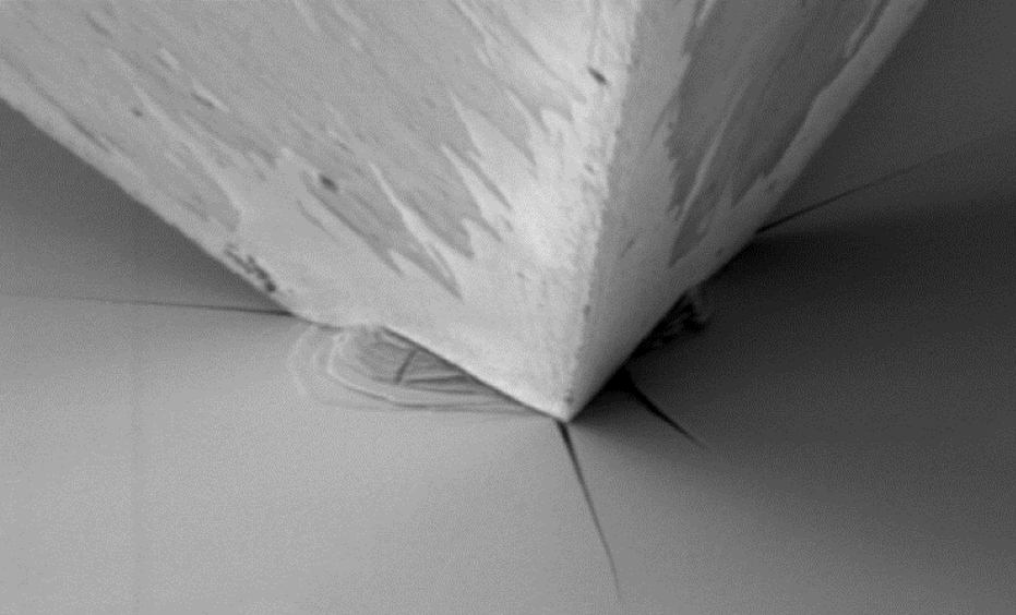
Advantages of Real-Time Contact Observation
Real-time contact observation takes nanoindentation techniques to new heights. Unlike conventional nanoindentation, the indentation area can be observed directly through an electron microscope allowing for the visualization of the contact area.5,6 This can lead to more reliable and repeatable experimentation. Furthermore, by viewing the indentation process, instantaneous feedback can be gathered on a material’s behavior, such as fracture onset, delamination, and time-sensitive behavior like viscoelasticity. Accordingly, researchers can identify changes in material properties that would otherwise be missed with conventional “post-mortem” analysis.7
Investigating High-Temperature Nanoindentation
High-temperature nanoindentation represents a specialized area within the field of nanoindentation, enabling precise characterization of a material’s mechanical behavior at elevated operational or processing temperatures. This involves subjecting the sample and indenter to temperatures as high as 800 °C, often conducted in a vacuum to prevent undesired atmospheric effects. The technique faces challenges like temperature drift and sample oxidation. However, with advancements like the Alemnis High-Temperature Module (HTM), high-temperature nanoindentation has become a standard method for studying temperature effects on material properties.8
Applications of Nanoindentation: High Temperature and Real-Time Contact Observation
High-temperature nanoindentation opens exciting possibilities for fundamental materials research. Its highly localized nature allows for an in-depth exploration of material behavior kinetics. This technique has been effectively employed to characterize a wide range of temperature-induced material effects, such as phase transitions in semiconductors like Si and Ge,9 stress-strain analysis of P91 steel,10 uncovering the atomic-level mechanisms of plasticity in solids,11,12 and crystallization behavior in bulk metallic glasses.13
High-temperature nanoindentation can also be combined with imaging techniques (e.g., SEM and TEM) and electrical measurements, enabling a comprehensive understanding of material behavior at the nanoscale.14 This has recently been demonstrated in additive manufacturing when investigating the temperature-dependent hardness of near-eutectic Ni-Nb,15 an Ni-based alloy that could be utilized in machinery components exposed to extreme loading conditions.16 Advances in these combined in-situ techniques permit real-time studies of temperature effects on microstructure and the intricate relationships between mechanical, electrical, and thermal phenomena at the nanoscale.[SL1]
Nanoindentation: A Small Measure with a Big Impact
Nanoindentation is a critical technique for understanding material properties at the nanoscale. Integrating real-time contact observation into nanoindentation techniques has significantly enhanced its effectiveness, allowing researchers to gain crucial insights into material behavior at unprecedented detail. With the development of high-temperature nanoindentation, the advantages of real-time observation hold immense promise for a wide range of applications in diverse industries. As research in this field continues to advance, real-time contact observation in nanoindentation will likely play a pivotal role in future materials science and engineering.
References and Further Reading
1. Nemecek J. (2012). Nanoindentation in Materials Science. http://dx.doi.org/10.5772/2829
2. Bhushan B, et al. (2016). Nanoindentation. Encyclopedia of Nanotechnology. https://doi.org/10.1007/978-94-017-9780-1_41
3. Peng Q. (2011). First-Principles Quantum Simulations of Nanoindentation. Nanoindentation in Materials Science. http://dx.doi.org/10.5772/48190
4. Sasmal S, et al. (2019). Nanoindentation for evaluation of properties of cement hydration products [chapter 7]. Nanotechnology in Eco-efficient Construction (Second Edition) Materials, Processes and Applications. https://doi.org/10.1016/B978-0-08-102641-0.00007-4
5. Cohen SR, et al. (2013). Dynamic nanoindentation by instrumented nanoindentation and force microscopy: a comparative review. Beilstein Journal of Nanotechnology. https://doi.org/10.3762/bjnano.4.93
6. Rzepiejewska-Malyska KA, et al. (2008). In situ mechanical observations during nanoindentation inside a high-resolution scanning electron microscope. Journal of Materials Research. https://doi.org/10.1557/JMR.2008.0240
7. Nowak J, et al. (2010). In-situ nanoindentation in the SEM. Materials Today. https://doi.org/10.1016/S1369-7021(10)70144-9
8. Alemnis [Online]. High Temperature Nanoindentation. Available at: https://alemnis.com/high_temperature_nanoindentation/ (Accessed on 27 July 2023)
9. Chavoshi SZ, et al. (2018). Temperature-dependent nanoindentation response of materials. MRS Communications. https://doi.org/10.1557/mrc.2018.19
10. Ruiz Moreno A, et al. (2020). Stress−strain curves and derived mechanical parameters of P91 steel from spherical nanoindentation at a range of temperatures. Materials & Design. https://doi.org/10.1016/j.matdes.2020.108950
11. Schuh CA, et al. (2005). Quantitative insight into dislocation nucleation from high-temperature nanoindentation experiments. Nature Materials. https://doi.org/10.1038/nmat1429
12. Choi I-C, et al. (2017). Thermally activated dislocation plasticity in body-centered cubic chromium studied by high-temperature nanoindentation. Acta Materialia. https://doi.org/10.1016/j.actamat.2017.08.026
13. Nieh TG, et al. (2004). Comparative studies of crystallization of a bulk Zr–Al–Ti–Cu–Ni amorphous alloy. Intermetallics. https://doi.org/10.1016/j.intermet.2004.04.011
14. Nili H, et al. (2013). In situ nanoindentation: Probing nanoscale multifunctionality. Progress in Materials Science. http://dx.doi.org/10.1016/j.pmatsci.2012.08.001
15. Jones MR, et al. (2023). Evidence of twinning-induced plasticity (TWIP) and ultrahigh hardness in additively-manufactured near-eutectic Ni–Nb. Journal of Material Science. https://doi.org/10.1007/s10853-023-08636-8
16. Vijay Reddy K, et al. (2020). Effect of Ni–Nb Metallic Glass on Moderating the Shock Damage in Crystalline Ni-Amorphous Ni62Nb38 Nanocomposite Structure: A Molecular Dynamics Study. In: TMS 2020 149th Annual Meeting & Exhibition Supplemental Proceedings. The Minerals, Metals & Materials Series. https://doi.org/10.1007/978-3-030-36296-6_85