Observing how materials respond to applied stress in their native state is fundamental to understanding their mechanical properties (creep deformation, fracture toughness, hardness, elastic modulus, etc.). Limited insights can be gained from structural and surface analysis of samples before and after a mechanical load has been applied, typically via indentation. However, this fails to yield accurate data regarding the real-time deformation behavior of samples under test.
In situ mechanical testing is the only way to observe the real-time mechanical performance of samples under applied loads. For instance, conducting nanoindentation in a scanning electron microscope (SEM) environment allows researchers to visualize key parameters of their mechanical tests, including the actual deformation mechanics of samples in real-time.
Read More: What Properties Can Be Measured By Nanoindentation?
In this article, Alemnis briefly explores how real-time materials characterization can be actualized using vacuum-compatible nanoindenters and complementary SEM-based imaging.
In Situ Mechanical Testing: Challenges & Solutions
Indentation is a common mechanical testing method used to explore the physical properties of different sample types (alloys, ceramics, polymers, etc.). The basic principle involves the application of a mechanical load via a diamond probe tip to determine a sample’s resistance to deformation. Typically carried out ex-situ, various indentation methods have been used to investigate the elastic moduli and hardness scales of materials as a function of load-depth curves. However, conventional indentation is unsuitable for in situ mechanical testing.
Because surface observations are made after the fact, all conclusions drawn from load-depth data that pertain to specific deformation mechanics within the material are largely speculative. This complication is compounded by the rise of nanomechanical testing based on sub-micro scale (μm) indentation. In situ mechanical testing subsequently requires a powerful imaging tool that can offer nanoscale observations of sample mechanics in real-time.
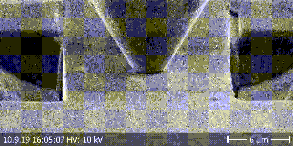
With far superior spatial resolution than optical light-based microscopy, SEMs have significantly shifted the goalposts of modern materials characterization. Prior to the onset of SEM, researchers were limited to nominal magnification ranges of up to 1000x due to the limited resolving power of visible light. A focused electron beam offers magnifying capabilities of up to 50,000x which yields extremely high lateral resolution ranging down to just a few nanometres (nm). Yet the limited geometries and vacuum pressures of sample chambers make it impossible to couple SEM imagery with conventional nanoindenters.
Small-scale, vacuum compatible nanoindentation modules are subsequently a prerequisite for in situ mechanical testing. This can yield a range of valuable results, providing accurate data regarding crack propagation, delamination, fracture onset, and more.
Real-Time Materials Characterization with Alemnis
Alemnis offers a unique solution for in situ mechanical testing of myriad sample types with real-time imaging via SEM. The Alemnis Standard Assembly (ASA) is a small footprint nanoindenter comprising a piezo actuated displacement head with an integrated sensor for completely closed-loop indentation testing. This module can be mounted and operated within the sample chamber of an SEM with sufficient space, enabling researchers to observe the real-time displacement of their samples down to a single nanometre.
If you would like to learn more about the unique Almenis solution for nanoindentation testing, read our previous blog post: What is a Nanoindenter?
We also provide custom mounting solutions and modifications for SEM integration. Contact a member of the Alemnis team today to learn about costing an ASA configuration with your SEM unit.