BEAM BENDING
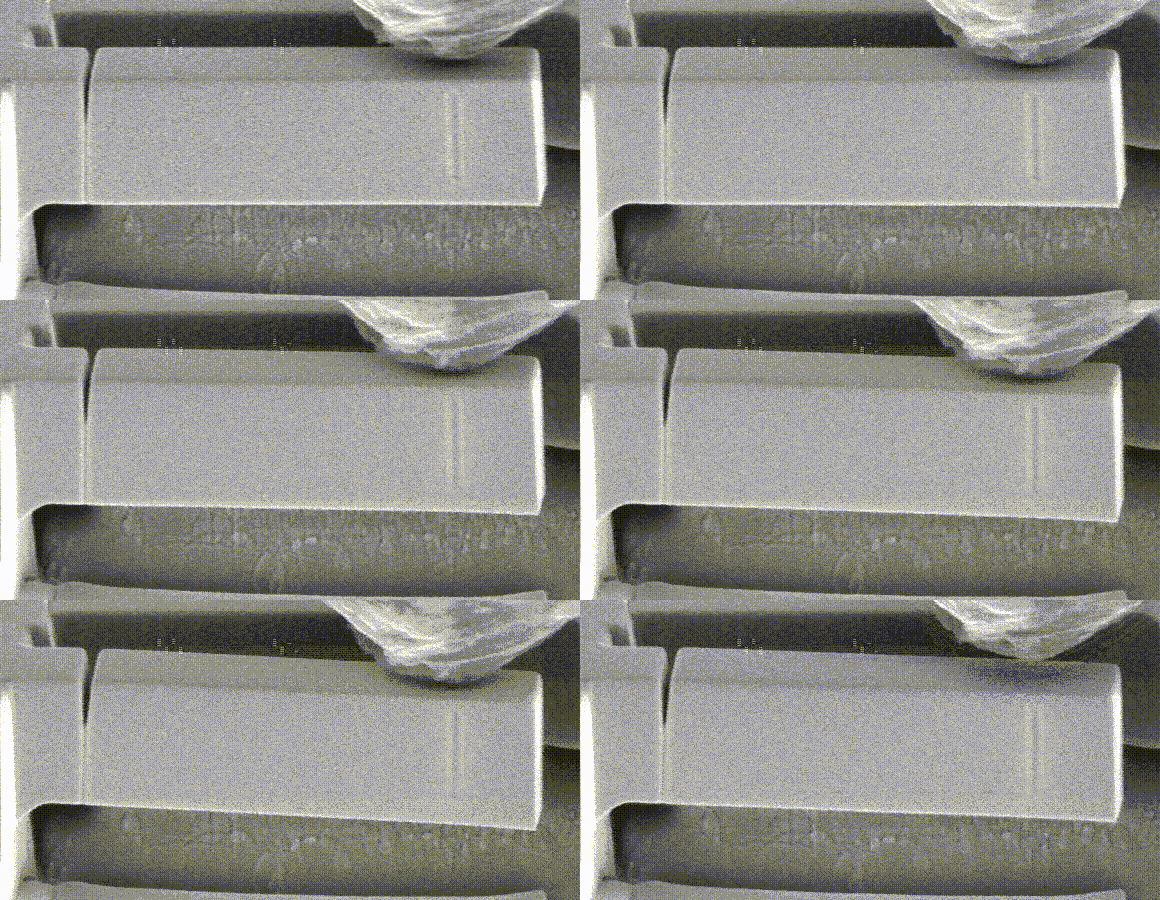
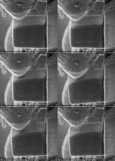
Beam bending experiments can be used to study size effects, time-dependent plasticity, fracture toughness, elastic modulus and for simulating MEMS structures (e.g., accelerometer beams used in capacitive airbag sensors). Typical microscale cantilever beams might have typical dimensions of 20 µm length and 5-7 µm in thickness and width. Displacement-controlled indentation tests are commonly made using a relatively blunt indenter (typically a spherical diamond indenter with radius 5 µm) to minimize deformation of the sample material under the contact zone.


The Alemnis Standard Assembly (ASA) is perfectly suited to beam bending experiments as it is a truly displacement-controlled instrument with a relatively large displacement range. In practice, this means that a beam can be deformed over many tens of microns for a correspondingly low measured applied load. This contrasts with standard nanoindenters which are often load-controlled and commonly have insufficient displacement range to fully deform certain beam geometries.
Beam bending tests are often combined with Electron Backscatter Diffraction (EBSD) analysis for a better understanding of elastic strains within the material as well as the distribution of accumulated geometrically necessary dislocations (GNDs).
It is also possible to apply nano-speckles to the beam by electron beam deposition of metals (e.g., platinum). The resultant array of small dots can be then used for Digital Image Correlation (DIC) of images acquired during the bend test, allowing the overall displacement field to be monitored.
Selected References
- H. S. Iyera, G. Mohanty, K. Stillera, J. Michler, M. Colliander, Microscale fracture of chromia scales, Materialia 8 (2019) 100465. https://doi.org/10.1016/j.mtla.2019.100465.
- B. N. Jaya, J. M. Wheeler, J. Wehrs, J. P. Best, R. Soler, J. Michler, G. Dehm, Microscale fracture behavior of single crystal silicon beams at elevated temperatures, Nano Letters 16 (2016) 7597–7603. https://doi.org/10.1021/acs.nanolett.6b03461.
- J. P. Best, J. Zechner, J. M. Wheeler, R. Schoeppner, M. Morstein, J. Michler, Small-scale fracture toughness of ceramic thin films: the effects of specimen geometry, ion beam notching and high temperature on chromium nitride toughness evaluation, Philosophical Magazine 96 (2016) 3552–3569. https://doi.org/10.1080/14786435.2016.1223891.
- J. Ast, G. Mohanty, Y. Guo, J. Michler, X. Maeder, In situ micromechanical testing of tungsten micro-cantilevers using HR-EBSD for the assessment of deformation evolution, Materials & Design 117 (2017) 265–266. https://doi.org/10.1016/j.matdes.2016.12.052.
- J. Ast, M. N. Polyakov, G. Mohanty, J. Michler, X. Maeder, Interplay of stresses, plasticity at crack tips and small sample dimensions revealed by in-situ microcantilever tests in tungsten, Materials Science and Engineering: A 710 (2018) 400–412. https://doi.org/10.1016/j.msea.2017.10.096.
- Y. Guo, J. Schwiedrzik, J. Michler, X. Maeder, On the nucleation and growth of {1122} twin in commercial purity titanium: In situ investigation of the local stress field and dislocation density distribution, Acta Materialia 120 (2016) 292–301. https://doi.org/10.1016/j.actamat.2016.08.073.
- C. Niederberger, W. M. Mook, X. Maeder, J. Michler, In situ electron backscatter diffraction (EBSD) during the compression of micropillars, Materials Science and Engineering: A 527 (2010) 4306–4311. https://doi.org/10.1016/j.msea.2010.03.055.
- X. Maeder, W. M. Mook, C. Niederberger, J. Michler, Quantitative stress/strain mapping during micropillar compression, Philosophical Magazine 91 (2011) 1097–1107. https://doi.org/10.1080/14786435.2010.505178.


